9.1 Boolean algebra, logic gate IC, and digital electronic techniques
Op-Amp ICs are electronic devices designed for processing analogue signals to perform mathematical functions like multiplications, differentiations, integrations, oscillations etc. Logic gate ICs, on the other hand, are digital electronic devices for processing (0 1) binary bits to perform digital computations based on binary Boolean expressions. Nowaday, logic gate ICs are far more important and sophisticated than Op-Amp ICs. Bearing this in mind, we understand that the infrastructure of Op-Amp IC and logic gate IC belong to two different categories of electronic technologies. They were developed roughly at about the same time but Logic gate ICs soon became more mature and advanced.
Logic gate ICs targeted at digital circuit designs and have wide scope of applications. Discrete (0 1) binary bit signals after processing by various logic gate ICs can have millions of commercial applications and are the key elements of digital appliances such as smart phones, computers, digital cameras, audio devices, TV sets, outdoor advertisement display board etc, let alone another even more important military and space applications. The past analogue audio and video technologies were completely replaced by digital video/audio coding formats such as MP3, MPEG 4, JPEG, AVI, FLV, DVD, MOV, WMV etc which all need indispensable logic gate IC circuitry for decoding.
(i) Binary Boolean algebra and binary digital logic
When we substitute decimal numbers 0 to 9 to an algebraic expression, we will obtain a resulting number. However, the world of digital computation has only two numbers, i.e. 1 (5 V) and 0 (0 V), we found we have to resort to another mathematical treatment which accepts only numbers 1 and 0. This kind of algebra was called “Boolean algebra”.
For a simple algebraic equation A + B = C, if we let A = 1, B = 2 we get C =3,if A= 2, B = 3 then C = 5, etc. However, if we illustrate it by Boolean algebra, we simply arrive at either A + B = A or A + B = B, as 0 and 1 are the only variables. Apply the finding to an electronic circuit, this means by inputting two terminals at the same time with (0 0), (0 1), (1 0) or (1 1) variables, since a binary (0 1) bit has 22 or 4 variations, we would expect the output to be either 1 or 0. Boolean expression logic derives “truth table” (Fig. 237):
| A | B | A + B = A |
| 0 | 0 | 0 |
| 1 | 0 | 1 |
| 0 | 1 | 0 |
| 1 | 1 | 1 |
| A | B | A + B = B |
| 0 | 0 | 0 |
| 1 | 0 | 0 |
| 0 | 1 | 1 |
| 1 | 1 | 1 |
(Fig. 237) Truth table
The above is mathematical concept. If we want to relate it to electronic technology, the best way is to use logic gate IC circuits. Boolean operator such as OR (+), AND (.) or NOT ( — ) can all be illustrated by respective logic gates.
(ii) Electronic logic gate
Electronic logic gate has two main categories: (i) early TTL (transistor – transistor
logic) and (ii) later CMOS (complementary metal oxide semiconductor).
| Types of logic gate | etc | ||||
| AND | NAND | NOT | OR |
(iii) TTL logic gate
As its name implies, TTL (Transistor-Transistor Logic), each unit of logic gate consists of two directly coupled npn transistors. Domestic TTLs are named as 74XX.
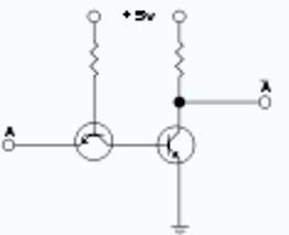
(Fig. 238) A unit of TTL inverter
As shown in Fig. 238, the emitter of the npn transistor on the left is used as an input (A) and as long as it is high (5V), small amount of current will flow through the collector (reverse active mode). This current activates the npn transistor on the right, conducting current to the ground, no p.d. is developed across the ground and the collector, pulling the output low (0V). When the input A is low, no current passes through to the right, the p.d. developed across the ground and the second npn collector is 5V. In this case, the output is high (Fig. 239).
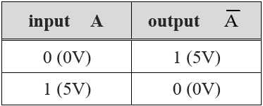
(Fig. 239) Truth table of Fig. 238
Logic gate ICs usually use DIP packaging. Each DIP IC has either (i) multi equivalent logic gates, like 7404 (Fig. 240) has 6 NOT logic gate units, or (ii) multi functional complex logic gates like CMOS 4511 (BCD to 7 segment) chip (Fig. 272).
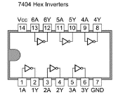
(Fig. 240) 7404 pin assignment
(iv) Complementary Metal-Oxide-Semiconductor (CMOS) logic gate
CMOS fabrication process manufactures another popular logic gate IC. It is made with both NMOS (n-type MOSFET)and PMOS(p-type MOSFET)on a circular silicon chip (Fig. 241). As NMOS and PMOS are characteristically complimentary, it is well known as CMOS.

(Fig. 241) A unit of CMOS logic gate
CMOS can be used in fabricating volatile memory such as RAM, micro-controller, micro-processor, CMOS optical sensor (digital camera), and other digital logic gate systems. CMOS semiconductor drains current only when the switch ON/OFF mechanism is activated. This outstanding advantage makes it consume much less power and hence little heat radiation. It became the most popular semiconductor component. Numbering of CMOS is in accordance with the 4XXX series.
At one time TTL and CMOS are at odds with each other. In comparison, TTL is faster but consumes more current than CMOS. As fabrication technique improved, respond speed of CMOS surpassed that of TTL. It also had an added advantage of resistor-free environment. Development of TTL lacked behind for a period of time. Today, TTLs were used mainly for education purposes and in simple digital circuits.
Power supply of TTL and CMOS is denoted by VDD or Vcc, usually 5 V. However, the differentiation voltage of the logic gate 1 (ON, high voltage) and 0 (OFF, low voltage) of TTL and CMOS are not the same. The threshold voltage range, that is the voltage of activating the output “1” state and the input “0” state of CMOS is different from that of TTL, leading to incompatibility of the two IC. For the same 5 V VDD, COMS circuits can drive TTL, but not the other way round.

Early TTL and CMOS cannot be directly coupled as shown in the above diagram. Nowadays, improved technology enabled manufacture of high-speed CMOS such as 74HCxxxx and low power Schottky such as the 74LS series, basically solved the compatibility problem. Fig. 242 illustrates how a CMOS NOT logic gate inverter works. Working principles of COMS and TTL can be viewed from the internet.
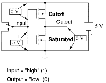
(Fig. 242) A CMOS inverter
Available logic gate chips all have respective namings. Large manufacturing companies like early FAIRCHILD or recent ones like MOTOROLA or TEXAS INSTRUMENT (TI) all provide detailed component specification charts and diagrams grouped as various manuals. Each company has its own product website for public viewing.
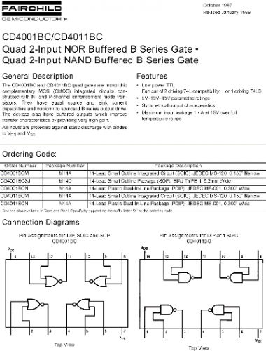
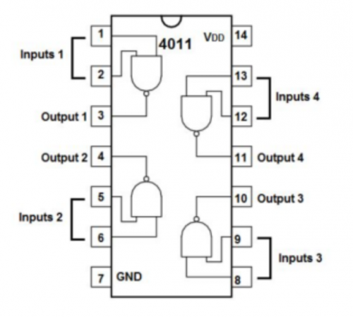
(Fig. 243) Description and pin arrangement for CMOS CD 4001 and CD 4011
CMOS Logic gate IC formed various electronic logic gates to illustrate seven binary Boolean operators AND、NAND、OR、NOR、XOR、XNOR and NOT (or INVERTER).
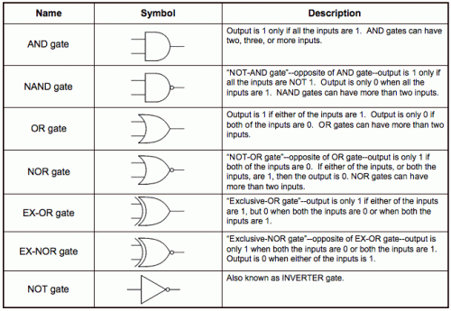
(Fig. 244) 7 Logic gates, their name, symbol and description
Their truth tables are listed below (Fig. 245):
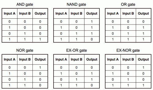 | INVERTER gate | |||||
|
(Fig. 245) Truth table of 7 electronic logic gates
The 7th logic gate, called as buffer, possesses no computational function. 0 V input results in 0 V output and 1 V input results in 1 V output. Its purpose is to improve input resistance of a device, notably in coupling Op – Amp ICs.
Summary:
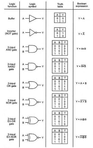
(Fig. 246) Various logic gates and the truth tables.
(v) Binary Boolean expression and truth table
Boolean expression | Logic gate and associated truth table |
A + B = A |  |
Boolean equation | Logic gate and associated truth table |
A + B = B |  |
(Fig. 248) Boolean expression A + B = B and associated truth table
(vi) Boolean algebraic logic, truth table and electronic logic gate
The greatest achievement of STEM applications was the implementation of digital electronic logic gate coding binary Boolean algebraic expressions. This opened the door to first generation followed by advanced programming of software and decoding by ever sophisticated hardware architecture. This development overwhelmingly demonstrated how beneficial was the integration of mathematics and technology to the betterment of human society through digital computation.
(a) 2 input binary bit (A B)
Inspecting the simplest binary Boolean expression A + B = A and A + B = B, we found that they can be expressed by a suitable combination of logic gates, transforming mathematics directly to technology. The + sign refers to input to any logic gate, not necessary only the AND gate. If we input the four variations of a binary bit (0 0), (1 0), (0 1) and (1 1), representing the four variations of the Boolean equation A + B = A to a single 2-input logic gate (i.e. AND, NAND, OR, NOR etc), we could not get the expected correct result of (0 1 0 1). It can only be accomplished by two coupled logic gates (OR plus AND etc) as illustrated below:
Boolean expression | Truth table | Logic gate combination (AND plus OR) |
| A + B = A |  |  |
Boolean expression | Truth table | Logic gate combination (OR plus AND) |
A + B = A |  |  |
Try again using the combination of (OR plus AND).
Boolean expression | Truth table | Logic gate combination (OR plus AND) |
A + B = B |  |  |
(1) Consider a more difficult case:
A + B = Always low (i.e. 0)
It is obvious that we haved to do something other than using (AND plus OR) or (OR plus AND) combinations. We try to put a NOT gate in between:
Boolean expression | Truth table | Logic gate combination (OR plus NOT plus AND) |
A + B = 0 |  |  |
or NOR plus AND |
(2) And: A + B = Always high (i.e. 1)
It can be simply solved by referring to example (1) using NOR plus NAND. Try it your- self.
(b) 3 input binary bit (A B C)
For 3 inputs such as (A + B + C), there are 23 or 8 binary variations. Consider the following logic gate combination:
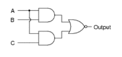
Try to find the corresponding binary Boolean expression.

(c) Standalone and combination logic gates
The seven 2 input logic gates mentioned earlier (Fig. 244, 245 and 246) are not independent and indispensable. Each one of them can be constructed with a suitable combination of other logic gates. Thus, we find building-blocks of logic gates that could generate all digital binary Boolean expression operators.
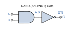
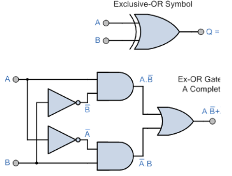
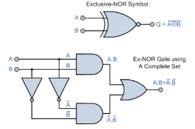
The set (AND, OR and NOT) is called a Full Set as the other four 2 input logic gates i.e. NAND, NOR, ExOR, ExNOR (including the buffer) can be built from the full set or any two of the full set, shown as follows:
 |  |
 |  |

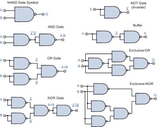
Using only one single logic gate to generate all other logic gates is called a Minimal Set. For example, a NAND gate is a minimal set:
(d) Commercial logic gate chips
In practice, all logic gates are commercially available as either CMOS or TTL chips, no one will try to build them from first principle by using transistors or semiconductors.
Chip manufacturing corporations like Texas Instruments, Motorola, Analog Devices etc had well been established since the past few decades. Most of the consumer products were standardized and remain in sale shelves unchanged, except for the advanced digital component parts (e.g. CPU or interface chips) necessary for the evergrowing personal computer markets. For example, the CD series of CMOS logic gate chips like 4xxx are used by all electronic circuit designers, they would not be outdated. Available commercial logic gate chip packages do not provide single units, multi-units of the same or mixed types are manufactured instead. Some available CMOS logic gate chips are illustrated in the following table:
IC | Description | IC | Description |
4081 | Quad 2-input AND | 4073 | Triple 3-input AND |
4011 | Quad 2-input NAND | 4023 | Triple 3-input NAND |
4071 | Quad 2-input OR | 4075 | Triple 3-input OR |
4001 | Quad 2-input NOR | 4025 | Triple 3-input NOR |
| 4070 | Quad Exclusive OR | 4082 | Dual 4-input AND |
4077 | Quad Exclusive NOR | 4012 | Dual 4-input NAND |
| 4000 | Dual 3-input NOR plus inverter | 4072 | Dual 4-input OR |
Thus, we found that a suitable combination of logic gates can implement basic Boolean logic expressions. In fact, the very basic step of each digital computation, irrespective of level of complexity, is actually done in this way, as each primary path is to decide whether a 0 1 pair should be 0 or 1. To summarize:

(e) A practical but sophisticated 4 input binary bit (A B C D) example
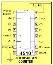
An often encountered example, but very complicated, is the hardware requirement of a BCD (Binary Coded Decimal) counter display. The following three tables outline the approach of displaying decimal numbers 0 to 9 by a 4 LED array, making use of readily available logic gate IC chips to perform complex Boolean operations. The one introduced below, CD 4510, suits the mentioned requirement.
Requirement | Truth table |
A digital device to display decimal 0 to 9 by a suitable combination of logic gates. A 2-bit LED array can have 22 or 4 possibilities, hence can display only 0 to 4 numbers, does not meet the demand. A 4-bit LED array has 24 or 16 possibilities. Hence it can display not only 0 to 9 but also other alphabets or symbols which belongs to a numbering system called hexadecimal. A clock is required to generate a chain of propagating square wave (pulse) with a frequency determined by the clock. A 4-bit (A B C D) truth table is required to match input (decimal number) and output (4-bit display). | 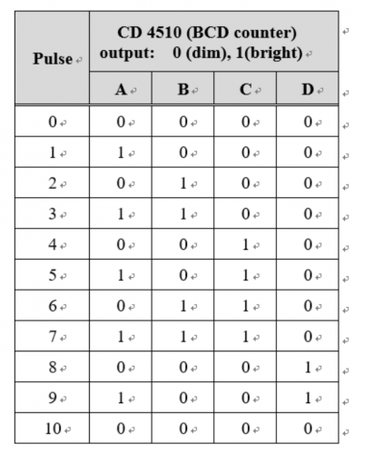 |
Logic gate circuit | ||
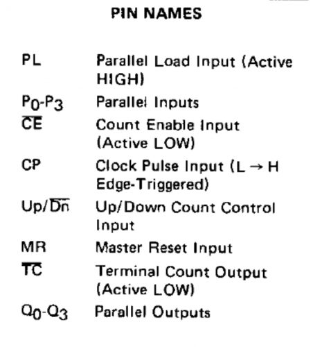
A complicated logic gate combination is required to do the job. # 0 indicated by (0 0 0 0) with a 4 LED array displayed as (dim dim dim dim) # 1 indicated by (1 0 0 0) with a 4 LED array displayed as (bright dim dim dim) # 2 indicated by (0 1 0 0) with a 4 LED array displayed as (dim bright dim dim) etc The required logic gate circuit is commercially available as a BCD 4 bit counter IC CMOS CD 4510, with a complex internal structure as shown below. | ||
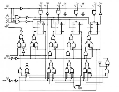 |  | |
CMOS CD 4510 BCD 4-bit counter | ||
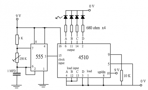
| The CD 4510 chip was designed for general digital circuit applications. Hence its pin arrangement accepts inputs of various digital computational signals. However, our simple job at this moment considers only the input clock or pulse signal and the four outputs (A B C D or Q0 to Q3), hence pins (1, 3, 4, 5, 8, 12 and 13) are all connected to ground. All other pins, i.e. pin 16 (VDD) is connected to + 9 V, pin 9, the reset pin, is tied to ground by a 10K resistor and pin 10 is connected to + 9V. The input pin 15 is linked to the clock, with timer 555 connected as an astable multivibrator which outputs (thro pin 3) a square wave pulse chain with a frequency around 3 Hz. The following diagram shows the actual wiring of set up on a breadboard. Topic 9.3 (Digital frequency counter) will give a more detailed description of the role played by CD 4510 as a counter. | ||
 |  | |
The following video clip illustrates how numerals 0 to 9 are displayed sequentially by a 4 LED array, all mounted on a breadboard.
CD 4510 BCD 4 bit output
Project (11 ):Using CMOS CD 4071 (Quad 2-input OR gate) and CD 4081 (Quad 2-input AND gate), verify the Boolean expression
Material: CD 4071, CD 4081, breadboard, 4.5V power supply, LED, 100 K W resistor (for decent intensity of LED light emission, try a lower value of resistance such as 50 K W), connecting wires, 3P4T selector
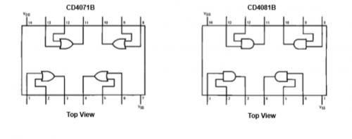
Steps: (1) Complete the following circuit wiring using the provided materials.
 |  |
 |
(Fig. 249) Boolean expression A+B = B and associated logic gate circuit
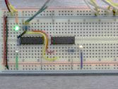
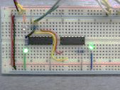
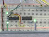
(2) Rotate the 3P4T selector so that A and B inputs are according to (0 0),(1 0),(0 1) and (1 1) variations. Observe the LED intensities of inputs A and B and also the output X.
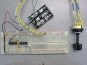 | 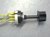 | 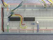 | ||||||
Photo of assembly | 3P4T selector (only 2 units are used) |
|
 |  |  |
|
|
| ||||||||||||||||||
(Fig. 250) Input A and B both with (0 0), (1 0), (0 1) and (1 1) and output displayed with lighted LED
A + B = B
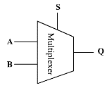
When to adopt the computation environment to A + B = A or A + B = B? This has to do with an electronic selector which is called a multiplexer. The truth table of a multiplexer is shown below:
S | A | B | Q | |
0 | 0 | 0 | 0 | A + B = A |
0 | 0 | 1 | 0 | |
0 | 1 | 0 | 1 | |
0 | 1 | 1 | 1 | |
| 1 | 0 | 0 | 0 | A + B = B |
| 1 | 0 | 1 | 1 | |
1 | 1 | 0 | 0 | |
| 1 | 1 | 1 | 1 | |
If S = 1, signal A and B will compute according to A + B = B, resulting in Q = B. If S = 0, signal A and B will compute according to A + B = A, resulting in Q = A. The above can be looked upon as computation expansion truth table of A + B = A or A + B = B, or as the simplest algebraic Shannon’ expansion in selecting 1 from 2.
Multiplexer has its own symbol (Fig. 251). 2 to 1 electronic selector is an analogue of a SP2T rotary selector (Fig. 252). A chip as such is also called as a three-state logic gate.
 |  |
| ||||||||
2 to 1 multiplexer | A rotary SP2T is an analogue of a 2 to 1 multiplexer | Shannon’s expansion truth table |
(Fig.251) (Fig.252)
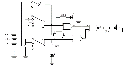
Project (12): Using CMOS CD 4011 (Quad 2-input NAND gate), simulate the Boolean expression option of A+ B = A or A + B = B by selecting 1 from 2
|  | |||||||||||||||||||||||||||||||||||||||
Material: CD 4011, breadboard, 4.5V power supply, LED, 100 KW resistor (for decent intensity of LED light emission, try a lower value of resistance such as 50 K W), connecting wires, 3P4T selector, SP2T selector.
Step:
(1) Complete the following circuit wiring using the provided materials.
 |  |
 | |
(Fig. 253) A + B = A or A + B = B 2 select 1 |
- Rotate the SP2T selector so that S through pin 13, is connected to gound i.e. 0 V (or S = 0).
- Rotate the 3P4T selector
- Select (A B) to be (0 0), record the light intensity of LED Q
- Select (A B) to be (1 0), record the light intensity of LED Q
- Select (A B) to be (0 1), record the light intensity of LED Q
- Select (A B) to be (1 1), record the light intensity of LED Q
- Connect S to + 4.5 V (or S = 1).
- Repeat the above steps.
Result: Complete the following table:
S | A | B | Light intensity of LED Q (bright = 1,dim = 0) | |
0 | 0 | 0 | A + B = ( ) | |
0 | 1 | 0 | ||
0 | 0 | 1 | ||
| 0 | 1 | 1 | ||
1 | 0 | 0 | A + B = ( ) | |
1 | 1 | 0 | ||
1 | 0 | 1 | ||
| 1 | 1 | 1 | ||
(vii) Frequency counter
Practical digital circuits of computers of course do not use manual selectors for switching various executing commands, instead multiplexers and clocks are used. Project (12) is only a simulation of how a multiplexer works. Actual multiplexers used in digital citcuits are much more complicated (internet self-study for details). Multiplexers need an external time clock to generate a continuous (0) and (1) OFF/ON state pulse chain for operations. Hence a clock provides a time base for computation. A clock is generally referred to as a frequency counter. Frequency counter used in computer hardware usually use piezo electric material such as quartz to act as an oscillator and provide square wave pulse chain with a precise frequency. A 1 GHz quartz oscillator generates109 5V square wave signals per second with an accuracy as high as one in 1/109 sec or 10-9 sec. Therefore, the higher the frequency, the more accurate will be the time base. Low frequency time base in consumer circuits, e.g. a few Hz to a few KHz normally do not use quartz oscillators, instead, an Op – Amp RC combination acting as an astable multivibrator (relaxation oscillator) or a CMOS inverting logic gate coupled with a capacitor or an even especially designed timer IC such as 555 is very suffix.
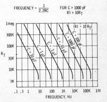
Op – Amp relaxation oscillator is a popular astable multivibrator for circuit designs (Fig. 228). Topic 8.3.2 (e) had already discussed its working principle. The following CMOS astable multivibrator using CD 4049 inverter logic gate IC (Fig. 254) has an output square wave frequency of f = 1/2.2 RC. If R = 100,000 W and C = 0.001 x 10⁻⁶ F, then
f = 1/(2.2 x 100,000 x 0.001 x 10-6) Hz or 4545 Hz。
Considering computational, resistor and capacitor value errors, the acceptable experimental value of the generated frequency is (+/-) 15% of 4545 Hz, or 4545 (+/-) 682 Hz
(Fig. 254) CD 4049 inverter oscillator |
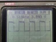
(Fig. 255) CD 4049 oscillator generating 5130 Hz square wave |
(viii) Digitization of distorted analogue signals
Digitization is a major means of eliminating interferences associated with analogue signals. When noise-free analogue sign is input to a logic gate buffer, i.e. 0 V input / 0 V output, 1 V input / 1 V etc, with a preset threshold voltage such that the digital output remains high, i.e. (1) when the input analogue voltage is above it and switched to low, i.e. (0) if the analogue voltage is lower than it, a digital binary (0 1) bit signal will form. Fig. 256 outlines the conversion (red line stands for the output digital signal while the green curve stands for the input noise-free analogue signal).
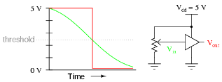
(Fig. 256) Analogue/digital conversion with a single threshold voltage
If the analogue signal is contaminated with noise signals, the output digital signal will not be the same as before. Consider a slow varying DC analogue signal with associated noise (green curve) is converted by the same means, the threshold barrier will have three break points instead of one, as shown in Fig 257. The output digital signal (red curve) will look like the diagram below (Fig. 257). Two digital signals instead of one are resulted.
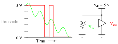
(Fig. 257) Threshold voltage appears twice, two digital signals instead of one
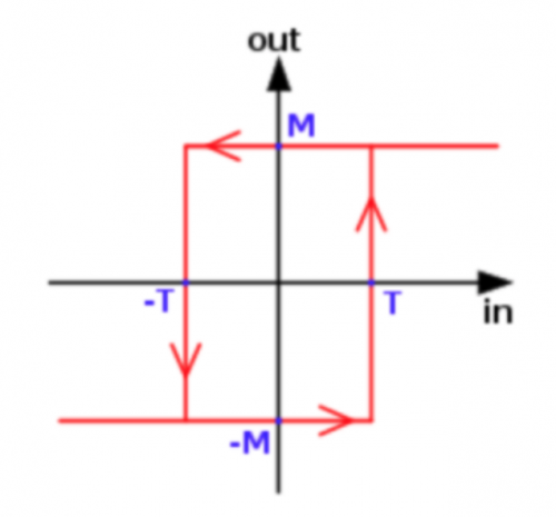
A Schmitt trigger is used to solve the above problem. The scheme is denoted by the diagram below. The central symbol is used to indicate the phenomenon of “hysteresis”, a term associated with the B-H curve for a ferromagnetic material. A Schmitt trigger is an Op – Amp comparator with positive feedback to the non-inverting input with two preset threshold voltages. The digital (0) and (1) states triggered by the lower and upper threshold voltages with time gap are determined by the applied analogue signal. This mechanism will be repeated according to the variation of the analogue signal. The to and fro operation as such follows a pattern which looks like a hysteresis curve.

In Fig. 258, when the analogue voltage is above the higher threshold, the (1) state is activated and the output stays at this state until the analogue voltage drops to the lower threshold which at that instant the output is instantaneously switched to the (0) state and remains there as long as the analogue voltage keeps low. In other words, the digital output remains high during the period of threshold voltage change. The result is formation of only one digital pulse instead of two as shown in Fig. 257.
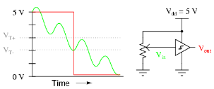
(Fig. 258) Distorted analogue signal and correction by a Schmitt trigger to give normal digital pulse
Schematic diagram of a Schmitt trigger (Fig 259). The horizontal and vertical axes are input voltage and output voltage respectively. T and −T are the switching thresholds, and M and −M are the digital output voltages. When T is exceeded, digital output is +5V and stays there until -T is reached which at that instant the digital output becomes 0V and stays there. The pattern will be repeated and forms a figure which looks like a B-H hysteresis curve. |
(Fig. 259) Transform curve of a Schmitt trigger |
Readers can look for more detailed information about the principle and applications of Schmitt trigger from internet resources.
9.2 Hardware, software, binary bit, byte, digital computation and personal computer (PC)
(i) Hardware and binary digital computing
Hardware of a personal computer consists of a physical, tangible assembly of electronic components including cabinet, central processing unit (CPU), monitor, keyboard, computer data storage, graphics card, sound card, speakers and motherboard. It becomes active only when the built-in operating system (OS) is activated and an organized binary digital logical set of instructions (software) are fed.
A binary bit (1 bit) has 21 or 2 variations, i.e. 0 and 1, practical use is just like a 2P1T selector when switched to the OFF or ON state. A binary 2 bit has 22 or 4 binary variations, i.e. (0 0), (0 1), (1 0) and (1 1). Practical use is for computational digital binary bit, widely used as the basic computational unit in computers. A binary 3 bit has 23or 8 binary variations, i.e (0 0 0), (0 0 1), (0 1 0), (0 1 1) (1 0 0), (1 0 1), (1 1 0) and (1 1 1). Binary 3 bit is seldomly used in digital computing. Recently, someone proposed binary 3 bit be associated with a digital version of the interpretation of ancient China’s 乾坤八卦和六十四卦 (Qiankun eight cases and Hexagrams) of 易經 (Yi Jing), exceeding the digitization, diagrammatic and symbolic frame of reference as opposed to traditional digital computation (internet search for details or pictured as Chinese ancient fortune teller using 3 copper coins inside a tortoise shell, representing heaven, earth and people). Binary 4 bit has 24 or 16 binary variations (hexadecimal). It was primarily used in early digital computing device, especially setting the standard for keyboard Latin Alphabet input, i.e. the ASCII (American Standard Code for Information Interchange) system.
The first generation of digital computation concept is based on binary 4-bit, involving a binary, octal, decimal and hexadecimal distribution scheme as illustrated below (Fig. 260):
Display | |||
Binary | Octal | Decimal | Hexadecimal |
0000 | 0 | 0 | 0 |
0001 | 1 | 1 | 1 |
0010 | 2 | 2 | 2 |
| 0011 | 3 | 3 | 3 |
0100 | 4 | 4 | 4 |
| 0101 | 5 | 5 | 5 |
0110 | 6 | 6 | 6 |
| 0111 | 7 | 7 | 7 |
1000 | 10 | 8 | 8 |
| 1001 | 11 | 9 | 9 |
1010 | 12 | 10 | A |
| 1011 | 13 | 11 | B |
1100 | 14 | 12 | C |
| 1101 | 15 | 13 | D |
1110 | 16 | 14 | E |
| 1111 | 17 | 15 | F |
(Fig. 260) Possible display of binary 4 bit distribution
It is obvious that 4-bit is incapable of relating the digital world with the daily human communication skills such as verbal and written specializations. 8-bit has 28 or 256 kinds of variations and is capable of distributing English alphabet A to Z, numerals 0 to 10, and other commonly used symbols such as -, >, <, / @ etc. All grouped as a set of ASCII characters. A programmed set of instructions (software) using human recognizable set of rules (programming language) is required to instruct the computer to execute specific demands.
Binary 4-bit can be encoded and decoded by machines only, it cannot be programmed with human set of rules. Hence the language used by binary 4-bit program is called “machine language” which has limited scope of general use. Binary 8 bit, or 1 byte, on the other hand, can primarily satisfy the construction of ASCII characters (Fig. 261, 262) and was used extensively in the early development of programming languages such as BASIC, FORTRAN etc.
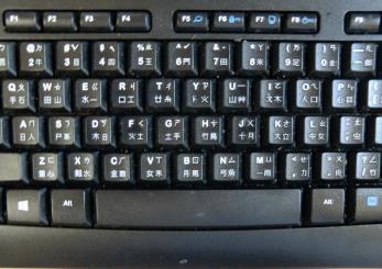
(Fig. 261) ASCII characters of keyboard
Limitation of the ASCII characters is that it can deal only with 26 letters of the Latin alphabet, Arabic numerals and English punctuation symbols. Hence it can be used only for English or American English display. Unicode (「統一碼」) characters was developed later which is applicable to other language systems. ASCII character set is widely used in programming languages. It is user-friendly and commonly adopted. (Internet search for more details).
Binary | Decimal | Hexadecimal | Graphic | Binary | Decimal | Hexadecimal | Graphic | Binary | Decimal | Hexadecimal | Graphic |
0010 0000 | 32 | 20 | (space) | 0100 0000 | 64 | 40 | @ | 0110 0000 | 96 | 60 | |
0010 0001 | 33 | 21 | ! | 0100 0001 | 65 | 41 | A | 0110 0001 | 97 | 61 | a |
| 0010 0010 | 34 | 22 | “ | 0100 0010 | 66 | 42 | B | 0110 0010 | 98 | 62 | |
0010 0011 | 35 | 23 | # | 0100 0011 | 67 | 43 | C | 0110 0011 | 99 | 63 | c |
0010 0100 | 36 | 24 | $ | 0100 0100 | 68 | 44 | D | 0110 0100 | 100 | 64 | |
| 0010 0101 | 37 | 25 | % | 0100 0101 | 69 | 45 | E | 0110 0101 | 101 | 65 | |
0010 0110 | 38 | 26 | & | 0100 0110 | 70 | 46 | F | 0110 0110 | 102 | 66 | F |
| 0010 0111 | 39 | 27 | ‘ | 0100 0111 | 71 | 47 | G | 0110 0111 | 103 | 67 | |
0010 1000 | 40 | 28 | ( | 0100 1000 | 72 | 48 | H | 0110 1000 | 104 | 68 | h |
| 0010 1001 | 41 | 29 | ) | 0100 1001 | 73 | 49 | I | 0110 1001 | 105 | 69 | |
0010 1010 | 42 | 2A | * | 0100 1010 | 74 | 4A | J | 0110 1010 | 106 | 6A | j |
| 0010 1011 | 43 | 2B | + | 0100 1011 | 75 | 4B | K | 0110 1011 | 107 | 6B | |
0010 1100 | 44 | 2C | , | 0100 1100 | 76 | 4C | L | 0110 1100 | 108 | 6C | l |
| 0010 1101 | 45 | 2D | – | 0100 1101 | 77 | 4D | M | 0110 1101 | 109 | 6D | |
0010 1110 | 46 | 2E | . | 0100 1110 | 78 | 4E | N | 0110 1110 | 110 | 6E | n |
| 0010 1111 | 47 | 2F | / | 0100 1111 | 79 | 4F | O | 0110 1111 | 111 | 6F | |
0011 0000 | 48 | 30 | 0 | 0101 0000 | 80 | 50 | P | 0111 0000 | 112 | 70 | p |
| 0011 0001 | 49 | 31 | 1 | 0101 0001 | 81 | 51 | Q | 0111 0001 | 113 | 71 | |
0011 0010 | 50 | 32 | 2 | 0101 0010 | 82 | 52 | R | 0111 0010 | 114 | 72 | r |
| 0011 0011 | 51 | 33 | 3 | 0101 0011 | 83 | 53 | S | 0111 0011 | 115 | 73 | |
0011 0100 | 52 | 34 | 4 | 0101 0100 | 84 | 54 | T | 0111 0100 | 116 | 74 | t |
| 0011 0101 | 53 | 35 | 5 | 0101 0101 | 85 | 55 | U | 0111 0101 | 117 | 75 | |
0011 0110 | 54 | 36 | 6 | 0101 0110 | 86 | 56 | V | 0111 0110 | 118 | 76 | v |
| 0011 0111 | 55 | 37 | 7 | 0101 0111 | 87 | 57 | W | 0111 0111 | 119 | 77 | |
0011 1000 | 56 | 38 | 8 | 0101 1000 | 88 | 58 | X | 0111 1000 | 120 | 78 | x |
| 0011 1001 | 57 | 39 | 9 | 0101 1001 | 89 | 59 | Y | 0111 1001 | 121 | 79 | |
0011 1010 | 58 | 3A | : | 0101 1010 | 90 | 5A | Z | 0111 1010 | 122 | 7A | z |
| 0011 1011 | 59 | 3B | ; | 0101 1011 | 91 | 5B | [ | 0111 1011 | 123 | 7B | |
0011 1100 | 60 | 3C | < | 0101 1100 | 92 | 5C | \ | 0111 1100 | 124 | 7C | | |
| 0011 1101 | 61 | 3D | = | 0101 1101 | 93 | 5D | ] | 0111 1101 | 125 | 7D | |
0011 1110 | 62 | 3E | > | 0101 1110 | 94 | 5E | ^ | 0111 1110 | 126 | 7E | ~ |
| 0011 1111 | 63 | 3F | ? | 0101 1111 | 95 | 5F | _ |
(Fig. 262) ASCII character set
In using a personal computer (PC), for a 10-bit character frame, when a key is pressed, the keyboard sends a start bit (low), followed by eight data bits, and one stop bit (high). For instance, pressing the “A” key will have it appeared on the screen. This means the PC is actually executing the (0100 0001) byte (Fig. 262, ASCII character set) by displaying a 8 x 8 pixel grid graphic as a result of Raster scan (Fig. 263).
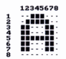 |
Character “A” in 8 x 8 Matrix by Raster Scan |
(Fig. 263) (0100 0001) matrix graphic display on screen as “A”
Thus, we can see the computer’s keyboard input mechanism aimed at a user-friendly and simple approach to carry out a variety of complicated execution commands necessary for the computer to function.
(ii) Programing language and software
(a) Domestic and Commercial software
A programming language is a vocabulary and set of grammatical rules for instructing a computer or computing device to perform specific tasks. It allows human beings use human languages to interact with computers by encoding specific and precise commands for execution, no error is allowed. It is classified as low level or high level languages. Low-level programming language is used for machine only, common people could not understand its meaning. It is also called “machine language”.
High-level programming language uses natural language elements. It is easier to read, write, and maintain, making the process of developing a program simpler and more understandable. In the 50s of last century, high-level programming languages used for software were developed. Like the popular (i) FORTRAN (FORmula TRANslator), mainly for the field of mathematics, (ii) COBOL (COmmon Business Oriented Language) for the commercial sector, (iii) BASIC (Beginner’s All-purpose Symbolic Instruction Code) for general use and (iv) LOTUS – 123, for spreadsheet usage. A spreadsheet is an interactive computer application for organization, analysis and storage of data in tabular form. At the beginning, these programming languages were used mainly for mainframe computers, but were soon highly commercialized and further developed as personal computers (PC) were globally manufactured. Java, C#, Python, Ruby etc are the currently well received programming languages suiting various purposes.
Software is a set of instructions, data or programs used to operate computers and execute specific tasks, usually completed by using different computing languages. CPU, the central processing unit of a vital component of hardware, experienced extremely fast development and the software associated with it also made tremendous progress each passing day. In the 70s, operating system (OS) of CPU all used DOS (Disk Operating System). Prevailing office software operating on DOS at that time were “WordStar” and “Word Perfect”. However, commanding DOS is a clumsy, unwise and lack of flexibility procedure. It was soon entirely replaced by a user-friendly desktop-ion and mouse-based MicroSoft “Windows” OS. Programming languages for earlier versions of “Windows” used Visual Basic and Visual Basic. NET. Latest development of “Windows 10” OS involved C, followed by higher Level languages like C#, CPP or Python. Notable Microsoft software is the ever-updating “Office” bundle which included the original document-based “Word”, spreadsheet “Excel”, presentation-based “PowerPoint” and e-mail facilitator “Outlook”. Later also included the “OneNote”, “OneDrive” and the video-based communication “Skype”.
(b) Industrial software
Industrial software is a collection of programs, processes and information for construction contractors in sectors such as engineering, mining, chemical, power, and manufacturing. Industrial software performs functions ranging from estimating, job costing, construction accounting and management and scheduling to highly specialized solutions for material design and other manufacturing processes.
The widely used basic software for engineering design is the MATLAB with additional Simulink package. MATLAB (“matrix laboratory”) was developed by MathWorks. It is very versatile and allows matrix manipulation, plotting of function and data, implementation of algorithms, creation of user interfaces, and interfacing with other programs. As of 2020, MATLAB has more than 4 million users worldwide. MATLAB users come from various backgrounds of engineering, science,and economics. Associate with industrial sector is a collection of popular software for design artists – AutoCAD, CorelDRAW and Photoshop. They had been well-received by general users for decades.
(c) Apps (abbreviation for software applications) for mobile smartphones
Entering the era of millennium, internet communication became a daily indispensable task for everyone. Hence drafting software or Apps suitable for mobile smartphones based on iOS or Android operating systems appears to be a must-do task for every IT worker. Unlike desktop computers which mainly use C, C++ and C#, the commonly adopted computing language for mobile phones are Java, Javascript, C#, C++, Python, PHP etc. They all support browsers such as Internet Explorer (IE), Google, Chrome and Firefox.
(d) Cloud computing
The term “Cloud computing” is a kind of metaphor, it carries no physical meaning. Cloud computing was developed quite recently. Cloud computing is the on-demand availability of computer system resources without direct active management by the user. Cloud-based storage makes it possible to save them to a remote database. Any ethernet desktop or wireless electronic device with suitable speed and memory and with internet connection can obtain cloud services as illustrated below:
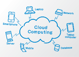
Types of Cloud Services include:
* Storage, backup, and data retrieval
* Creating and testing apps
* Analyzing data
* Audio and video streaming
* Delivering software on demand
Broadly speaking, there are three types of Cloud Cervices: (i) software-as-a-service (SaaS), (ii) infrastructure-as-a-service (IaaS), and (iii) platform-as-a-service (PaaS). (SaaS) involves the licensure of a software application to customers. Licenses are typically provided through a pay-as-you-go model or on-demand. This type of system can be found in Microsoft “Office 2016” or “365”, which is totally different from traditional CD ROM-based “Office” softwares. Server-free availability is offered by using IaaS, while web-hosting service is a typical use of PaaS.
Cloud computing users can check their e-mail on any computer and even store files using services such as Dropbox and Google Drive. Store or retrieve Instagram photos through the cloud by smartphones become a current fashionable activity. Because of its high mobility, cloud computing is especially useful in mobile AI applications like IoT, unmanned driving, drones, robots etc.
By the way, free webmail services like Gmail, Yahoo mail and Hotmail are provided by web browsers. They do not fall into the same category as Cloud services.
(iii) Exponentially increased development of binary byte architecture
Although binary 8-bit byte programmed words can be converted to ASCII characters for computer input, a byte length as such is just a basic requirement for CPU operation. As fabrication of CPU became more advanced and sophisticated in terms of speed and volume of memory handling, byte architecture also experienced exponentially increased development. First came the introduction of 16-bit 2 byte binary word instructions, then the 32-bit 4 byte and now the implementation of 64-bit 8 byte configurations, all aimed at coupling with the ever-renewing CPU architectures. Related programming languages are thus available in rich varieties as mentioned earlier.
To conclude, the innovation of digital electronics and technology is closely linked to binary Boolean algebraic expressions, a vivid demonstration of technology and mathematics are closely related as lips and teeth。Far-reaching applications of digital electronics is the most successful example of STEM achievements.
9.3 Software and hardware forward / reverse engineering (internet information-based)
(i) Software forward / reverse engineering
As its name implies, forward engineering refers to the process of producing product from raw materials. Just the opposite, reverse engineering is the process by which a targeted man-made object is dismantled to reveal its designs, architecture and to extract knowledge from the object. It is usually done for the purpose of duplicating or enhancing the performance of the object.
Software source code, instruction, compiled code and binary object code
A computer works only when the software couples with the hardware precisely. In layman’s term, software tells the computer hardware exactly when and how to work. To put the entire business into reality, one has to technically follow the exact steps right from the source (software) to the end (computer hardware). The process is called software forward engineering.
Forward engineering of computation starts with choosing a suitable computational language and write an error-free program compatible with the OS of the hardware architecture. For example, a simple program in C language for showing on the screen the equation “3 + 8 = 11” is drafted as follows:
Line | |
1 | #include |
2 | |
3 | int main() |
4 | { |
5 | int a, b, c; |
6 | a = 3; |
7 | b = 8; |
8 | c = a + b; |
9 | printf(“%d + %d = %d\n”, a, b, c); |
10 | return 0; |
11 | } |
The header (standard input output as header) is an instructional jargon associated with C language which means standard input from the keyboard and standard output shown on the screen. The line int main() declares the main function. These instructions are collectively called as “source code”. Computer hardware does not recognize programs in C language or any high-level languages, it accepts only 0s (0V) and 1s (5V) binary bits. Therefore there is a need to change these high level languages to a lower level language (e.g., assembly language, object code, or binary machine code) by a compiler to create an executable program. The overall result is mountains of 0s and 1s of binary bits are directed precisely to various destinations of the hardware infrastructure to perform the desired and complicated logic gate operations.
To amend the above program, say change the equation to 5 + 7 = 12, you simply change a to 5 and b to 7. If the source code is lost, you have to start from square one, find out the language employed and rebuild the program to meet the need or optimize it. That is reverse software engineering. However, source code for a complicated program, like “Windows 10”, is more than a half terabyte in size, and uses more than 4 million files (Fig. 264). Even programming experts cannot figure out at which lines of the program should amendments be made, if they are not provided with the source code.

(Fig. 264) File size of “Windows 10”
In order to amend a program whose source code had been lost, one has to do a software reverse engineering process. Software reverse engineering involves reversing a program’s machine code back into the source code. It is necessary to retrieve the source code of a program so that improvements of the performance of a program can be made. It also serves the purpose of fixing bugs (correct errors in the program) and identifying malicious contents in a program such as implanted viruses. Reverse engineering for the purpose of copying or duplicating programs constitute copyright violation. Software reverse engineering is very complicated. It is not only costly and may not obtain desirable results.
(ii) Hardware forward and reverse engineering
IC and SoC (System-on-a Chip) chipset industry
Hardware reverse engineering involves taking apart a device to see how it works. For example, if a processor manufacturer wants to see how a competitor’s processor works, he can purchase a competitor’s processor, dismantle it, and then make another processor similar to it. However, this process is illegal in many countries. In general, hardware reverse engineering requires a great deal of expertise and is colossally expensive. Why not buy it from a dealer?
Positive engineering of chipset manufacture is broadly classified as two types: (i) IDM (Integrated Design and Manufacture) and (ii) OEM (Original Equipment Manufacture).
(1) Integrated Design and Manufacture (IDM)
Letter M of the abbreviation IDM carries the key meaning of the term. Design and other procedures are not regarded as product manufacture. IDM means the manufacturer does the design, fabricating the wafer, packaging and testing of IC all by the company itself. A traditional IDM owns its own branded chips. Intel company is a kind of IDM which manufactures “Intel CPU”.
IDM was widely adopted in the early days of semiconductor industry when IC circuitry complexity was low. Nowadays, when mobile smartphones become indispensable, “Intel” or other IDM corporations share only a fraction of the electronic computational appliance market by manufacturing desktop main components, the main market goes to the more advanced and complicated chipset installed in smartphones. For smartphone manufacturers, it is impractical and cost prohibitive for one company to handle all the processes. A more ecosystem environment where (i) the design (software support critical), (ii) lithographic etching, (iii) silicon substrate wafer making, (iv) packaging and (v) testing are allocated to different companies. The manufacturing sector of this kind of semiconductor industry, i.e. process (ii) and (iii) is called OEM (Original Equipment Manufacture).
(2) Original Equipment Manufacture (OEM)
(a) EUV lithography and OME
For a desktop computer motherboard, you find the processor CPU, graphic card, RAM slot etc are positioned separately (Fig. 265). However, a mobile phone hardware cannot afford such space extravagance. The central chipset has to contain a number of vital circuitry components and must be very small. Hence the “brain” of a smartphone is a SoC chipset (System-on-a-Chip) which integrates almost all of these components into a single tiny silicon chip. Along with a CPU, an SoC usually contains a GPU (a graphics processor), memory, DSP (digital signal processor), Video encoder/decoder, USB controller, power management circuits, modems for wireless signals (WiFi, 3G, 4G LTE, 5G, Bluetooth and so on) (Fig. 266).
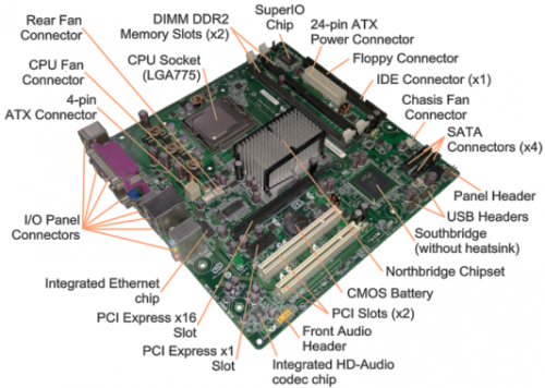 | 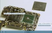 |
(Fig. 265) Layout of a desktop motherboard | (Fig. 266) A smartphone SoC chipset (Kirin970) |
After designing the complicated circuitry, what processes are required to manufacture these sophisticated smartphone SoC chipsets? Two separate levels of technologies were involved: (i) nm scale (i.e.10-9m electromagnetic wave) light lithographic etching technology and (ii) embedded component OEM (Original Equipment Manufacture), 代工生產). Sadly, as of today, there is only one “company” in the world which is capable of manufacturing EUV (Extreme Ultraviolet,13.3–13.7 nm wavelength range) lithographic machine (Fig. 267) that can undertake the highly precise craftmanship of EUV irradiation of silicon oxide/silicon substrate and met the 7 nm technology accuracy demand (as of 2019). The EUV lithographic etching process is summarized by the following flow chart:
 |  |  |  | |||
(i) Preparation of wafer | (ii) Application of photoresist | (iii) Alignment of photomask | (iv) Exposure to EUV |
 |  |  | ||
(v) Development and removal of photoresist exposed to EUV | (vi) Etching of exposed oxide | (vii) Removal of remaining photoresist |
Steps (iii) to (vi) have to be repeated according to complexity of the design.
The dominating manufacturer of EUV lithographic machine is called ASML (Advanced Semiconductor Materials International) Holding of the Netherlands. The “company” is technically supported by a number of multinational enterprises and financially supported by end-users. The “company” sells only technology through lithographic machines and not chipset products. Manufacturer and users are the core stakeholders.
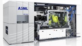
(Fig. 267) An ASML EUV lithography machine as a 7 nm SoC chipset starter
In 2019, along with shipment to Samsung and Intel, half of the exported 26 sets of ASML EUV lithographic machines were shipped to TSMC (Taiwan Semiconductor Manufacturing Company Ltd., 台積電) for OEM (Original Equipment Manufacture), 代工生產) SoC chipset 7 nm wafers (晶圓片) of Apple’s A14 Bionic for iphone 12, Huawei (華為)’s Kirin 990 5G for Mate 30 or the Qualcomm (高通)’s Snapdragon 865 for Samsung Galaxy S20. These tiny silicon-layer architecture has a transistor density in the order of 100 million per mm2.
No single multinational giant smartphone manufacturer can do away with such vigorous (lithographic etching – OME) IT bureaucratic practice and capable of undergoing self forward engineering to manufacture 4G or 5G smartphone SoC chipsets. Along with such thinking, reverse engineering of a smartphone SoC chipset simply does not work.
“Early bird catches the worm”. As long as smartphone SoC chipsets are based on micro-silicon fabrication architecture, ASML firmly holds the bottle-neck of SoC chipset OME.
(b) Dry etching – Reactive Ion Etching (RIE) and Deep Reactive Ion Etching (DRIE) technology (Internet search)
Apart from chemical (wet) treatment of removal of material on substrate used in EUV lithographic etching, Reactive-ion etching (RIE) is another etching technology used in microfabrication. RIE is a type of dry etching. It uses chemically reactive plasma to remove material deposited on wafers. The plasma is generated under low pressure (vacuum) by an electromagnetic field. High-energy ions from the plasma targeted at the wafer surface and react with it. Etching rate of RIE is not competitively high. An improved technology is the Deep Reactive-Ion Etching (DRIE). It uses double plasma beam instead of one. It is a highly anisotropic etching process used to create deep penetration, steep-sided holes and trenches in wafers/substrates The recognized “Bosch technology” used a repeating pattern of Passivation—etching—passivation—etching—.
How are microchips made
(3) IDM style of SoC manufacture
IDM was adopted for low transistor-density chip manufacture. Very high transistor-density chips, notably the SoC chipset, were manufactured by separate enterprises involving designing, lithography, etching, packaging and testing. This was not of financial or trade problems, but because of the heavily patent-loaded techniques and the extremely high level of technological demands which cannot be easily possessed by any single giant multinational enterprise and that resulted in the development of the OEM industry and the associated microfabrication companies.
Quite recently (2019 onwards), because of political reasons, China and America first exchanged trade tariff barriers and then as China rapidly expanded the scale of development of 5G network infrastructures, both locally and internationally, US fear that they are experiencing the start of a situation of lacking behind in the field of advanced micro-electronic technology. Interruption of the OME manufacturing chain is one way of screwing up China’s 5G development. Hence Huawei found it impossible to approach ASML and TSMC for their Kirin SoC chipsets. In 2020 Huawei, however, gave a back thrust by purchasing 120 million Dimensity (天璣) chips from MediaTek Inc. (MTK, 聯發科技, also rely on TSMC for OEM) as stockpile for the coming two years’ 5G smartphone consumption.
To respond, China 2020 started the “Dual economic circulation” tactic (mainly target at recovery after the worldwide economic downturn due to the new coronavirus Covid-19 pandemic) and one of the facets is to aim at nationally-based IDM of nm level SoC chipsets, like boosting the development of SMIC (Semiconductor Manufacturing International Corporation), making OEM of SoC chipset enterprise state owned. As China becomes economically and technologically viable, a long-term endeavour to overcome its weakness in lithographic technology is apparently on schedule. In 2020, the Chinese Academy of Sciences (CAS) with affiliated Suzhou Institute of Nano-Tech and Nano-Bionics (SINANO), developed a different kind of direct laser nano level lithographic technology (or maskless lithography) other than the EUV photoresist masking lithography adopted by ASML. It is hoped that IDM of nm level SoC chipsets could be rolled out to meet market demand of sophisticated smartphones in a matter of few years.
As of 2020, the initial IDM chip manufacturing giant enterprise, the Intel company, announced the plan of 7 nm chip IDM without out sourcing help from OEM such as TSMC or Samsung. Unfortunately, the endeavour was not sailing on calm sea.
(4) “Carbon-based logic gate” and “carbon molecule-based logic gate” development
The newly exploring “carbon-based” electronic logic gate technology (internet search) may one day provide an even superior alternative for silicon-based SoC chipset manufacture. In 2020 CAS teams of China announced success in the fabrication of graphene-based high-speed semiconductor and single crystal graphene wafer. In view of the fact that SoC chipset fabrication will come to a halt when 2 nm silicon-based SoC chipset starts to roll out for the smartphone market as no existing or future technologies are capable of handling 1 nm or less silicon lithographic chips (in terms of field running stability), carbon (or graphene)-based SoC chipset manufacture is expected to be the most likely player in the post silicon-based SoC chipset era. From an entrepreneur point of view, once the manufacturing line was established on silicon microfabrication, there will be no way to switch to carbon microfabrication, as all installation had been geared to that technology, even if it faces a dead end.
China’s endeavor in carbon-based chip development
A long expected “carbon molecule-based logic gate circuitry” is hoped to be able to implant into human organs without interface for medical use, invoking a new chapter of medical treatment development. (Revise p.32: The mysterious human brain memory)
9.4 Electronic project: Digital frequency counter
Digital numerical display reminds us the variations of 0 to 9 Arabic numerals. After acquiring the skills mentioned in the previous chapters, we are in a position of building a frequency counter of this nature, i.e. a digital frequency counter. Complete circuit can be divided into 3 modules, all mounted on a breadboard for easy assembly.
(1) The first module: A clock for generating time base.
(2) The second module: Match the generated digital (0 1) pulse from the first module with a CD 4510 BCD 4-bit counter to output BCD (Binary Coded Decimal) 4-bit signal.
(3) The third module: Employ CD 4511, a BCD to 7-Segment Decoder chip to change the input BCD 4-bit signal to abcdefg 7-bit output to drive a 7-segment LED for numeral display.
Modularized assembly of the completed circuit
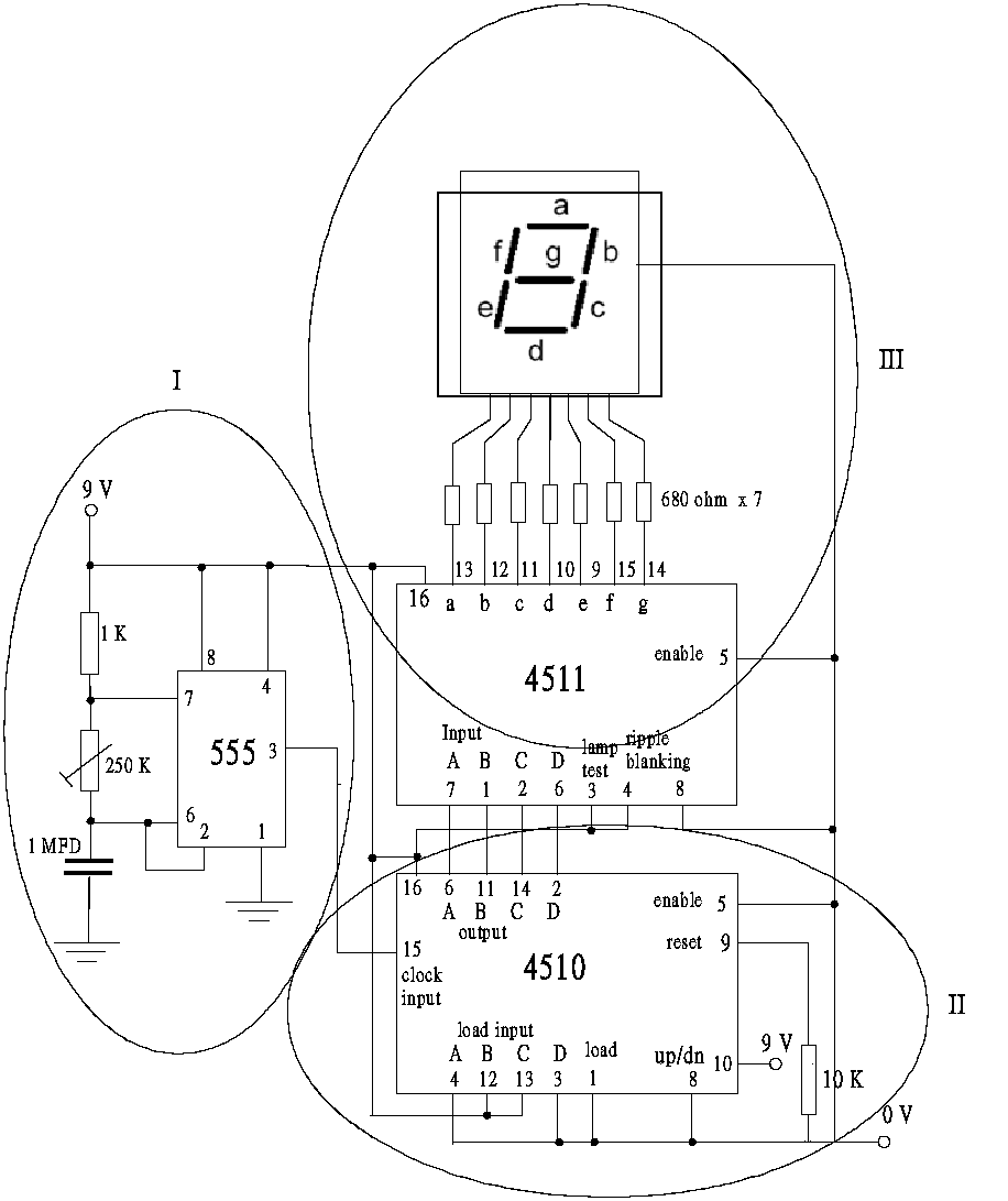 |
| (Fig. 268) Modularized 0 to 9 numerical counting display |
(i) Module (1) – IC 555 astable multivibrator
First construct a time base. IC 555 is a popular timer specially designed for waveform signal generation. The circuit needs an astable multivibrator to generate a frequency of a few Hz square wave pulse chain. The first module uses IC 555, 1K (Ra), 250 K (Rb) variable resistor and 1mF (C) capacitor to function as an astable multivibrator. The free-running oscillation has a frequency of f = [1.443/ (Ra + 2Rb) (C)] Hz.
Mechanism of frequency control is by varying the value of Rb instead of C. By substituting Ra = 1000 W,Rb = 250 KW variable resistor, C = 1mF into the circuit as shown in Fig. 269, frequency of bright/dim periodic cycles of the LED is calculated to be 1443 Hz to 2.88 Hz.
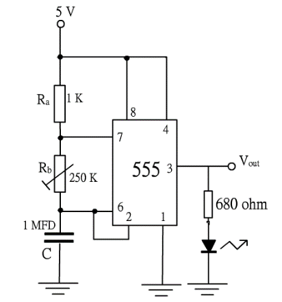
(Fig.269) Circuit to illustrate the bright/dim periodic cycles of the LED
Note:
(a) Not advisable to completely assemble the whole frequency counter circuit at the beginning. Should assemble it module by module. Oscillation part of Module (1) by timer 555 (Fig. 269) should be tested if oscillation had actually occurred. View the YouTube video clip.
(b) Power supply of IC 555 is 5V, not 9V. A 9V supply can burn the LED and affect the frequency generated.
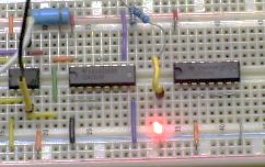
555 oscillator
(ii) Module (2) – add CD 4510 BCD 4-bit counter
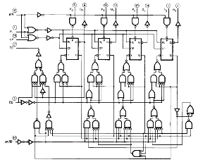
(Fig. 270) Internal structure of CD 4510
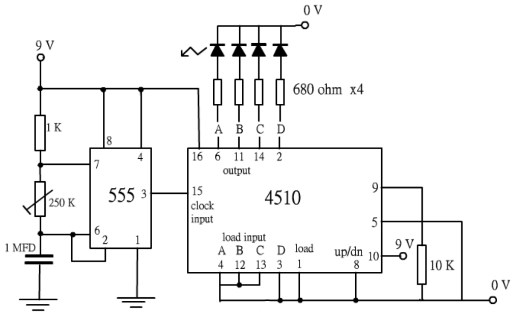 |
| (Fig. 271) ABCD output connected to 4 independent LED |
CD 4510 BCD 4-bit ouput
Connect Module (1) and Module (2) by joining pins 3 and 4 of 555 to pins 15 and 16 of CD 4510 respectively. Complete the circuit as shown in Fig. 271. CD 4510 is a BCD counter. It will decode the input signal into BCD 4-bit (A B C D) output. The corresponding truth table is illustrated as follows:
| Pulse | CD 4510 (BCD counter) output, 0 represents dim 1 represents bright | |||
| A | B | C | D | |
| 0 | 0 | 0 | 0 | 0 |
| 1 | 1 | 0 | 0 | 0 |
| 2 | 0 | 1 | 0 | 0 |
| 3 | 1 | 1 | 0 | 0 |
| 4 | 0 | 0 | 1 | 0 |
| 5 | 1 | 0 | 1 | 0 |
| 6 | 0 | 1 | 1 | 0 |
| 7 | 1 | 1 | 1 | 0 |
| 8 | 0 | 0 | 0 | 1 |
| 9 | 1 | 0 | 0 | 1 |
| 10 | 0 | 0 | 0 | 0 |
(iii) Module (3) – convert BCD input to abcdefg 7-bit output
The next stage is to convert BCD 4-bit to abcdefg 7-bit output for diving the 7 segment LED to display numerals 0 to 9. Truth table is shown below:
| BCD input | 7 segment output | |||||||||
| A | B | C | D | a | b | c | d | e | f | g |
| 0 | 0 | 0 | 0 | 0 | 1 | 1 | 1 | 1 | 1 | 0 |
| 1 | 0 | 0 | 0 | 0 | 1 | 1 | 0 | 0 | 0 | 0 |
| 0 | 1 | 0 | 0 | 1 | 1 | 0 | 1 | 1 | 0 | 1 |
| 1 | 1 | 0 | 0 | 1 | 1 | 1 | 1 | 0 | 0 | 1 |
| 0 | 0 | 1 | 0 | 0 | 1 | 1 | 0 | 0 | 1 | 1 |
| 1 | 0 | 1 | 0 | 1 | 0 | 1 | 1 | 0 | 1 | 1 |
| 0 | 1 | 1 | 0 | 0 | 0 | 1 | 1 | 1 | 1 | 1 |
| 1 | 1 | 1 | 0 | 1 | 1 | 1 | 0 | 0 | 0 | 0 |
| 0 | 0 | 0 | 1 | 1 | 1 | 1 | 1 | 1 | 1 | 1 |
| 1 | 0 | 0 | 1 | 1 | 1 | 1 | 0 | 0 | 1 | 1 |
The conversion needs software support. Because the circuit is so often used in digital designs, IC chip manufacturers simply turned it into a hardware, using CMOS fabrication to produce CD 4511 BCD to 7 segment IC for the consumer market. It soon became very popular, as a lot of digital designs involve numerical display.
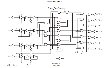
(Fig. 272) Internal structure of CD 4511
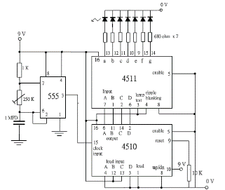
(Fig. 273) abcdefg 7-bit output to 7 independent LED
(iv) Module (3) contd. – output abcdefg 7-bit to 7 segment LED digital display
Finally, we have to convert the abcdefg 7-bit output to drive a 7 segment LED. Available 7 segment LEDs are classified as either (i) the common anode type, or (ii) the common cathode type. Displayed colour is either red or green.
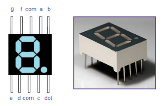 | 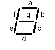 |
| 0.56” common cathode 7 segment LED pin arrangement is as follows: pin 3 or pin 8 to be connected to ground or 0V. Supply voltage of 3V when connected to pin 1 or pin 8 will light up segment e, pin 2 will light up segment d, pin 4 segment c, pin 5 for the dot, pin 6 for b, pin 7 for a, pin 9 for f and pin 10 for g. | |||||||||
| 7 segment output | Numerical display | ||||||||
| a | b | c | d | e | f | g | |||
| 0 | 1 | 1 | 1 | 1 | 1 | 0 | 0 | ||
| 0 | 1 | 1 | 0 | 0 | 0 | 0 | 1 | ||
| 1 | 1 | 0 | 1 | 1 | 0 | 1 | 2 | ||
| 1 | 1 | 1 | 1 | 0 | 0 | 1 | 3 | ||
| 0 | 1 | 1 | 0 | 0 | 1 | 1 | 4 | ||
| 1 | 0 | 1 | 1 | 0 | 1 | 1 | 5 | ||
| 0 | 0 | 1 | 1 | 1 | 1 | 1 | 6 | ||
| 1 | 1 | 1 | 0 | 0 | 0 | 0 | 7 | ||
| 1 | 1 | 1 | 1 | 1 | 1 | 1 | 8 | ||
| 1 | 1 | 1 | 0 | 0 | 1 | 1 | 9 | ||
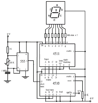
(Fig. 274) Complete circuit for the digital frequency counter displaying numerals 0 to 9
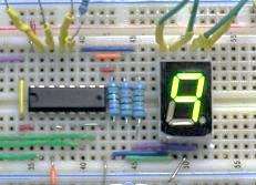
(Fig. 275) abcdefg 7-bit driving a 7 segment LED display
Real time square wave pulse signal output is shown as follows:
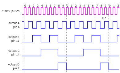
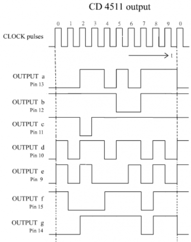
The above diagram can be interpreted as follows:
0 pulse :Oscillation starts CD 4510 outputs (0 0 0 0),CD 4511outputs (0 1 1 1 1 1 0)
1st pulse:CD 4510 outputs (1 0 0 0),CD 4511 outputs (0 1 1 0 0 0 0)
2ndpulse:CD 4510 outputs (0 1 0 0),CD 4511 outputs (1 1 0 1 1 0 1)
3rd pulse:CD 4510 outputs (1 1 0 0),CD 4511 outputs (1 1 1 1 0 0 1)
4th pulse:CD 4510 outputs (0 0 1 0),CD 4511 outputs (0 1 1 0 0 1 1)
5th pulse:CD 4510 outputs (1 0 1 0),CD 4511 outputs (1 0 1 1 0 1 1)
6th pulse:CD 4510 outputs (0 1 1 0),CD 4511 outputs (0 0 1 1 1 1 1)
7th pulse:CD 4510 outputs (1 1 1 0),CD 4511 outputs (1 1 1 0 0 0 0)
8th pulse:CD 4510 outputs (0 0 0 1),CD 4511 outputs (1 1 1 1 1 1 1)
9th pulse:CD 4510 outputs (1 0 0 1),CD 4511 outputs (1 1 1 0 0 1 1)
The whole scheme is summarized as follows:
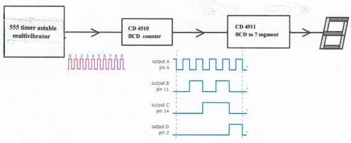
Note: CD 4510 pin 8 (up/down) provides the mechanism of 0 to 9 continuous consecutive display. That is if pin 8 is tied to the ground, ascending display results. On the other hand, if pin 8 is switched to the supply voltage, i.e. 9V, continuous descending display will occur.
0 -9 upcounting
9 – 0 downcounting
0 – 9 varying speed counting
Adjusting the variable resistor 250 KΩ controls the speed of counting.
Principle of digital display of pulse is not an easy study for beginners, as it cannot be illustrated by a single simple circuit. Because of this, all digital circuits should be analyzed as mentioned above. In fact, all digital circuits, regardless of complexity, can be scaled down to just a combination of ON/OFF electronic switch (logic gate) coupled with a time base made complicated according to various designs.


