8.1 Understand usage and command sketching of basic electronic components and circuits
| Name | Symbol | Function | Remark | |||
| Connecting wire | Electric wire | For electrical conduction, usaully copper wire enclosed with plastics. | ||||
| Wires connected | Circuits thro and connected | |||||
| Wires not connected | Circuits not connected | |||||
| Switch |  |
SPST toggle switch | (OFF), circuit not connected, (ON), circuit connected | |||
 |
1P2T toggle switch | Select one out of two terminals | ||||
 |
Push ON/OFF switch | Circuit connected when pushed on | ||||
| Ground |  |
Connected to ground | 0 p.d., normally connected to the (-) pole of batteries or the Vee of an IC chip. | |||
| Connected to chassis | Physically connected to the metal chassis. 0 p.d., used for electrical shock protection | |||||
| Resistor |   |
Fixed resistor | Major use as current limiter, minor use as heater. A very popular component. | |||
  |
Variable resistor (3 pin) | Use to hand-adjust current, a very popular component, allowed current usually not more than 0.5A. | ||||
| Variable resistor (3 pin) | ||||||
 |
Variable resistor (2 pin) |
Actual 2-pin component is not common (e.g. LDR), usually taken for granted as 3-pin version. |
||||
 |
Variable resistor (2 pin) | |||||
| Capacitor |   |
Fixed capacitor | Usually used in non-linear circuit designed for oscillation or in digital circuits as time clock component. Small value (1pF – 1mF), suitable for low or high voltages. A very popular component. | |||
 |
Electrolytic capacitor | Store positive or negative charges, mainly used for filter after rectification. High capacity (1mF – 5000mF). Provides positive and negative poles. Range of voltage application is some what limited. A popular component. | ||||
 |
Variable capacitor | Used for radio frequency resonance selection in early radio sets. Very small capacity, seldomly used nowadays, except for some fine adjustment circuits. | ||||
| Inductor |  |
Air core coil | Usually called as coil, used in high radio frequency waves, very small current flow. | |||
 |
Iron core coil | Called as “choke”, used in low frequency AC power supply. Its function is to limit high frequency current and allow low frequency current to pass through | ||||
| Transformer |  |
Step-up or step-down AC voltages | AC current only, not suitable for DC current. | |||
| Relay | Electrical switch | Used in circuits as non-manual switch | ||||
| Power supply |  |
AC power supply | H.K. domestic/commercial AC single phase power supply is 220V, 50Hz. Industrial power supply is AC three-phase 380V. | |||
 |
DC battery, dry cell, portable power supply |
Voltage range: 1.5V,3V,9V or 12V Types: zinc/carbon, alkaline, lithium ion, rechargeable |
||||
| Meter |  |
Ammeter, measure current |
Types: DC meter/AC meter Range: A, mA, mA |
|||
 |
Voltmeter, measure voltage |
Types: DC meter/AC meter Range: V, mV, mV |
||||
| Bulb | Tungsten filament (illumination) | High power dissipation, current consumption at least 50 mA, mainly used as pilot lamps but today largely replaced by LEDs. | ||||
| Diode | Rectification, detection | Allow positive cycles and cut off negative cycles. | ||||
| LED | Illumination | Diode fabricated with special dye, emits near monochromatic electromagnetic wave, very low power consumption, very popular. | ||||
| Zener diode | Voltage regulation | A special kind of diode, used for voltage regulation. | ||||
| TRANSISTOR | PNP |  |
Amplifies input signals. A lot of drawbacks. | Base input, collector connected to earth or 0V. Search for theory of voltage amplification through the internet. | ||
| NPN |  |
Amplifies input signals. A lot of drawbacks. | Base input, collector connected to power supply. Search for theory of voltage amplification through the internet. | |||
|
Darling-ton transistor |
 |
Power amplification of signal | Usually used in power amplification part of an amplifier. | |||
| IIC INTEGRATED CIRCUIT | Linear |  |
Operational Amplifier (Op-Amp) | Analogue integrated circuits, tenths and hundreds of various transistors coupled with resistors and capacitors to form an integrated circuit (IC). Linearly amplifies input analogue signals. Voltage gain ranges from 0 to indefinitely large. Can perform various mathematical functions like addition, division, differentiation, integration, etc. hence its name operational. | ||
| Voltage regulator | Analogue integrated circuits. Stabilizes input voltage and maintain a long term lower than input regulated voltage. Short-circuit protected. | |||||
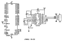 |
Interface | Built-in complicated analogue and digital circuits. A/D or D/A converter assumed. Key component of computer hardware. | ||||
| Logic gate |  |
TTL (NOR gate) | All digital circuits, operation according to truth table. Compatible with other logic gate devices. Slightly higher current consumption. TTL logic gates have 74XX 4-digit coding (military uses 54XX). | |||
 |
TTL (AND gate) | All digital circuits, operation according to truth table. Compatible with other logic gate devices. Slightly higher current consumption. TTL logic gates have 74XX 4-digit coding. (military uses 54XX). | ||||
| Other logic gates like OR, NAND, XOR、XNOR are commercially available | ||||||
 |
CMOS | All digital circuits, basically consists a pair of complimentary MOS transistors. Operation according to truth table, use the same symbol as TTL. Compatible with other logic gates. Small consumption of current. Coding of CMOS follows with a 4-digit number 4XXX. Early models were not compatible with TTLs, e.g. output of TTL cannot be directly fed to a CMOS. However. Later models of TTLs were greatly improved, CMOS and TTL became compatible. | ||||
| Antenna | Receive radio waves | Became obsolete. Nowadays, electronic devices use VHF or UHF. Reception sensitivity is high and there is no need to use antenna. | ||||
8.2 Simple formulae calculations (complicated induction calculations not included)
(A) V = iR (Ohm’s law)
Although a simple formula, could be a bit complicated when applied to real situations.
(a) Voltage (V) / potential difference (p.d.) / electromotive force (e.m.f.) of a cell
Broadly speaking, voltage and p.d. are basically the same thing, p.d. is a bit professional though. A difference is found in dry cells. We use e.m.f. instead of voltage of a cell. When a voltmeter registers voltage reading, a very small amount of current is taken from the signal source (i.e. a cell) so as to enable the voltmeter to operate. If the p.d. can be measured without consuming current from a cell, then the measured p.d. = e.m.f. of the cell.
The following illustrates the concept of e.m.f. of a cell:
| The voltage, or p.d., measured across a and b of a cell = iR where R is the internal resistance of the voltmeter. Unfortunately, we often take it for granted that the measured p.d. = e.m.f. of the cell. Since e.m.f. of a cell is defined as the p.d. measured without taking current from the cell, and this is made possible if the internal resistance R of the voltmeter is very large, so large that almost no current is allowed to pass through or i ~ 0. In short, e.m.f. of a cell refers to the p.d. measured with almost no current consumption which can be achieved by using a high resistance voltmeter. | 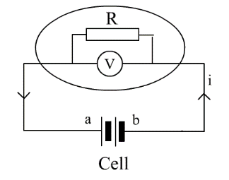 |
Digital multi-meter (DMM) is usually used to measure e.m.f. of dry cells. The internal resistance of most DMM is 10 MW or more. This value of resistance would not load the source by taking away appreciable amount of current for measurement,i.e i ~ 0. For example, when using a 10 MW DMM to measure the p.d. of cell and obtain a value of 1.10 V. Current through the DMM is 1.10/107 A or 1.10 x 10⁻⁷ A which is almost 0 A. In this case, the cell can be said to have an e.m.f. of 1.10 V. For more accurate measurement, professional voltmeter with internal resistance much higher than 10 MΩ should be used.
(b) Addition and subtraction of voltages
(+)(-)(+)(-)(+)(-) … addition applies
(+)(-)(-)(+)(+)(-) … subtraction applies
Complete the following tables:
| (i) |  |
|
||||||||||||||||||||||||||||||||||||||||
| (ii) |  |
|
||||||||||||||||||||||||||||||||||||||||
| (iii) | Ω |
|
||||||||||||||||||||||||||||||||||||||||
(B) Resistor combinations
(i) Connected in series:
 | i = i1 + i2 |
(ii) Connected in parallel:
| R = R1 + R2 | i = i1 = i2 |
The concept of resistors connected in parallel does not only find in actual soldered circuits, some hidden practical parallel “resistors” are also important in circuit design considerations.
Practical examples
(1) E.m.f of a cell
E.m.f. of a Daniell cell is 1.10V with an internal resistance of 500Ω. Calculate the voltage of the cell measured by (a) a moving coil ammeter with an internal resistance of 10,000Ω and (b) a DMM with an internal resistance of 10 MΩ.
Note: The internal resistance of commercial dry cells , like1.5 V,9 V etc are pretty low, in the order of 0.5Ω.
| (a) | 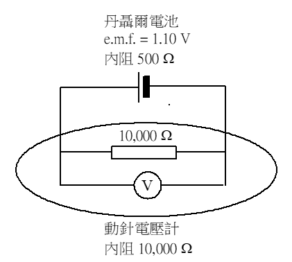 | * | The cell and the voltmeter are in fact connected in parallel. |
| * | |||
| * | |||
| * | Total resistance = 476.2 W | ||
| * | Available current = (1.10/500) A = 0.0022 A | ||
| * | p.d. across voltmeter = (476.2 x 0.0022) V = 1.048 V | ||
Measured p.d. = 1.048 V (e.m.f. = 1.10V) | |||
| (b) | 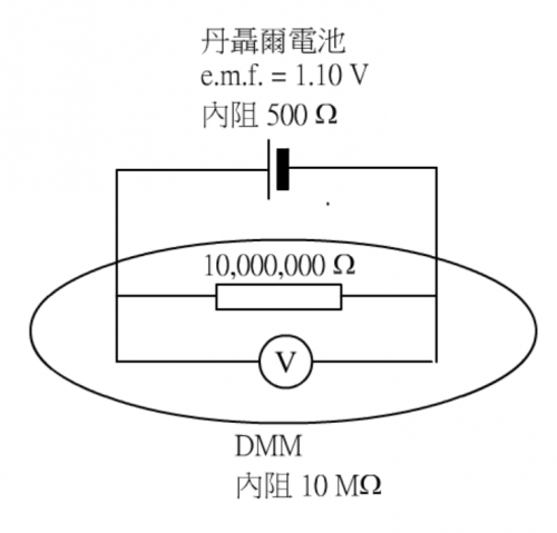 | * | The cell and the voltmeter are in fact connected in parallel. |
| * |
| ||
| * | Total resistance = _______ W | ||
| * | Available current = (1.10/500) A = 0.0022 A | ||
| * | p.d. across voltmeter = (_____ x 0.0022) V =_______V | ||
Measured p.d. = _______V (e.m.f. = 1.10V) | |||
From the above findings, one should use _____________ for cell e.m.f. measurements. Cells with ________ internal resistance can deliver higher current and e.m.f.
| Measuring instrument | Assumption | |
| Cell e.m.f. | High resistance voltmeter/DMM | Zero cell internal resistance |
(2) Input loading and internal resistance of instrument
A simple flow chart of instrumentation:
| Instrument | |
 | |
| Probe outputs weak DC signals | DC analogue amplification to about 2V |
Roughly analyzed as:
 | or |  |
The whole instrumentation circuit can be looked upon as a parallel combination of the signal source resistance and the internal resistance of the instrument. When a probe which generates a signal of e.m.f. = iSRS is connected to the instrument which itself does not generate any e.m.f., the resulting resistance is in fact a parallel combination of RS and RL. Signal source current iS will be shared by the loading resistor RL and becomes less. Thus, the testing e.m.f. will be less than the expected isRS. This situation is not desirable and will lead to inaccurate measurement. Technically, we say the “instrument loads the source signal”. If the instrument has a high input (internal) resistance, e.g. >10MΩ. loading phenomenon is not so severe and the measurement is more accurate. The situation is very similar to cell e.m.f. measurement, in which a high resistance voltmeter is recommended to measure cell e.m.f.
To summarize:
| Resistance of probe (RS) | Internal resistance of instrument (RL) / consequences | |
| High | Low | |
| High | Sensitivity of instrument not affected, but vulnerable to noise interference. | Some current will be drawn from the source to the instrument, resulting in a smaller value of e.m.f. generated by the probe. Measured e.m.f. is not the expected e.m.f. Sensitivity of the instrument is decreased. |
| Low | Sensitivity of instrument not affected, no noise problem. | Sensitivity of instrument may be slightly or not affected |
Thus, the golden rule of selecting probe and instrument is:
A probe with low resistance and an instrument with high input resistance.
(3) Fine adjustment of output voltage
Output voltage of circuits sometimes do not meet desired requirements. For example:

(Fig. 193) Variation of output voltage from 0 to 5V

(Fig. 194) Variation of output voltage form 0 to 1V
As shown by the above diagrams, the Op-Amp amplifies an analogue input signal to 3V. However, the following coupled circuit can only handle input voltages less than 1V, a single variable resistor R of course can do the job (Fig. 193), but with a little modification, replacing R by a series combination of R1 and R2 (Fig. 194) can improve the situation.
Let R2 = 5KΩ variable resistor. An output less than 1V can be calculated as follows:
i(R1 + 5000) = 3
i(5000) = 1
Solving the above equations, we have R1 = 10,000Ω。
If the desired voltage Vout = 0.75V,using circuit shown in (Fig. 193), it can be obtained within a range of 0 – 3V. However, using circuit as shown in (Fig. 194), the voltage range becomes 0 – 1V. Obviously, the latter is more accurate.
(4) Input/output calculations

(Fig. 195) Inverting input amplification circuit using an Op-Amp
The following formulae used for calculation will be discussed in more details in Topic 8.3. (Fig. 195) is a standard inverting input amplification circuit using an Op-Amp IC.
| Vout = -Vin ( |
Value of R3 equals to the parallel combination of R1 and R2.
![]()
Let the input voltage = 0.7V,measured p.d. across points (1) and (2) is 0.037V. calculate a voltage value for the IC output.
| Voltage (V) | Polarity | IC output (V0ut = ? V.) | ||
| (1) / (2) | 0.037 | (1) / (2) | (+) / (-) | + 0.293V |
| (2) / (3) | (- -) 0.037 x | (2) / (3) | (-) / (+) | |
| (3) / | ? + (0.37) + (0.037) = 0.7 ? = 0.293 | (3) / | (+) / (0) | |
Vout = 0.293 V
Thus, if a positive p.d. is applied to an Op-Amp connected for inverting input amplification, the resulting output voltage is not amplified but decreased. Only negative p.d. input will result in positively gained output.
R3 is not involved in calculation, its function in the circuit design will be discussed in Topic 8.3.2b.
(C) Combination of capacitors
Capacitors, if grouped together, are normally connected in parallel and seldomly connected in series.
 C = C1 + C2
Unlike resistors, circuits concerned with capacitors connected in parallel are not common. They are usually used singly.
Two types of commonly used capacitors: Electrolytic capacitor and (Fig.196) and ceramic capacitor (Fig. 197)
 | 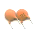 |
| (Fig. 196) Electrolytic capacitor | (Fig. 197) Ceramic capacitor |
| Electrolytic capacitor: | Bigger size, leads with polarity. The long one stands for positive terminal and the short one is the negative terminal. Limited applied voltage, if labelled as 25V 1000μF, the applied voltage should not exceed 25V DC, otherwise it will be damaged |
| Ceramic capacitor: | Smaller size, leads have no polarity. They can withstand high voltages, e.g. > 400V DC. Values lie between 1pF to 1mF. Almost all used in RC oscillation and non-linear circuits. Frequencies generated by RC oscillators normally are not less than 10Hz, they are governed by the simple formula of f =1/RC (refer to the next sessiom). |
(D) Oscillation circuits
Analogue circuits normally do not need timing platform as amplitudes of input analogue signals vary automatically with time preset by the frequencies of the signals. On the other hand, digital circuits must have a time platform for the (0 1) binary bits to be properly processed, otherwise these discrete bits carry no specific purposes. Analogue circuits involving linear Op-Amps can be designed to operate in a non-linear manner to carry out mathematical functions like integration or oscillation. Nearly all oscillation circuits involve RC coupling with working principle based on charging/discharging of capacitors. Oscillators generate pulse signals which serve as a platform for time base.First of all, an introduction to the charging and discharging phenomenon is required.

As shown on the left, current flowing through the capacitor accumulates electric charges on both sides. P.d. across the capacitor increases as shown on the right.

When the circuit is switched off, charges on both sides of the capacitor will neutralize, or called as discharge, resulting a drop in p.d.
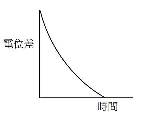
If the switch on/switch off action continues non-stop, a saw-tooth like pulsing waveform is generated.
Practical reality of course would not employ such manual method. Op-Amp or logic gate as well as quartz oscillation are used instead. Before we go into some details about IC oscillation circuits (Topic 8.3.2), it is helpful to know how a one-shot oscillation is produced.
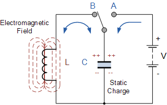
Inductor and current interaction:
Magnetic field is established when current passes through an inductor. Established magnetic field in turn induces the inductor and generates a back e.m.f., producing a reverse current. Recall Topic (7) i – inductor.
One-shot wave-form oscillation:
Referring to the above diagram, when switched to position A, the capacitor is charged. When switched to position B and stays there, the capacitor discharges. Conventional current flows through the coil and generates a magnetic field which immediately induce a back e.m.f. and generates a reverse current. The reverse current charges the capacitor again, in fact cancels the stored charges and then reverse the polarity. The next stage will be the capacitor with reversed parity induces the coil again and generates a next back e.m.f. which brings the entire situation back to square one but with much reduced intensity. This goes on repeatedly without limitation until the phenomenon eventually dies. If the capacitor is connected in series with a resistor, a one-short oscillating voltage will be developed as follows:
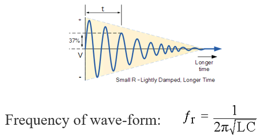
Sustained wave-form oscillator:
To enable oscillation sustainable, it seems that if the “push-pull” (positive e.m.f.- back e.m.f. – positive e.m.f.- back e.m.f….) mechanism of the one-shot counterpart can be maintained by some means, sustainable oscillation is feasible. That is exactly the basic principle of RC Op-Amp oscillation. The charge and discharge process of RC coupling, which governs the frequency of the generated signal, is maintained by a positive and negative feedback resistor network of an Op-Amp connected in a comparator mode. Usually, resistors are used instead of inductors, mainly because of availability and cost. In fact, owing to high design demand, ICs aiming at oscillation purposes are available, notably timer 555. For Op-Amp oscillators, the Relaxation Oscillator design is the mostly adopted circuit for small scale square wave pulse generation. Its working principle and application will be discussed in some details in Topic 8.3 (Practical Analogue Circuits). Basic formula for frequency calculation of such circuit is represented by
f = (![]() ) Hz.
) Hz.
Simple substitution of values of R and C will obtain the designed requirement. (Topic 8.3.2 Applications of linear Op-Amp ICs part (e) has detailed description).
8.3 Practical Analogue Circuits
(For self study, please view the website: https://www.allaboutcircuits.com)
8.3.1 Operational amplifier and ideal/non-ideal Op-Amp
* Purchasable Op-Amps are all non-ideal Op-Amps
* All related calculations are based on ideal behavior
* Circuit designs are required to eliminate the non-ideal behavior of practical Op-Amps
(a) Operational amplifier
Operational amplifier (Op-Amp) is the most important chip for analogue signal circuits. As its name implies, it can perform linear amplification and other mathematical function operation. Experienced people simply call Op – Amp as “Linear”. The following diagram shows an Op-Amp:
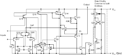
Internal structure of Dual Op-Amp LM 358 (each chip has two identical units):
(Fig.198) Structure of one unit of LM 358)
Because it has two inputs: (i) IC (+) pin and (ii) IC (-) pin, there are two methods of input: (i) differential input and (ii) common-mode input.
Practical considerations of Op-Amp in instrumentation
The following aspects are based on an ideal Op-Amp.
(i) Differential input
An Op-Amp has 2 inputs. It can accept two signal sources simultaneously. When the (+) input is connected to signal source and the (-) input connected to the other signal source, this method is called differential input and the amplifier under such condition is called differential amplifier (Fig. 199). Differential amplifiers are usually employed for instrumentation purpose, like input probes of thermistor or LDR used as part of a Wheatstone bridge sensor for accurate temperature and light intensity measurements.
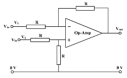
(Fig.199) A typical differential amplifier
(ii) Common-mode input
As most instruments are dealing with single signal sources, the common-mode input is the most prevailing input method of Op-Amps. When one of the the input terminals of the Op-Amp is connected to ground (0V), and the other connected to the signal source, we say it is connected in the common-mode way. As far as DC amplification is concerned, there are two major methods of design, namely (i) inverting amplifier (Fig. 200) and (ii) non-inverting amplifier (Fig. 201). More details of the two methods will be discussed in Topic 8.3.2.
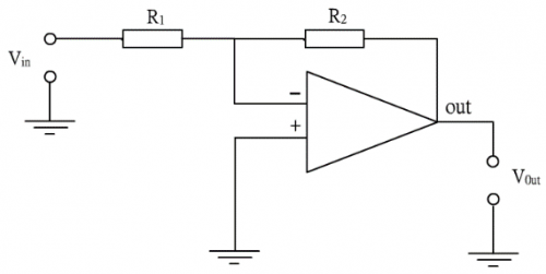 | 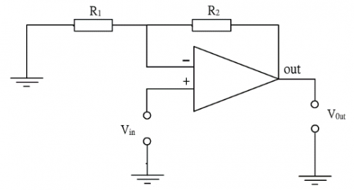 |
| (Fig. 200) A typical Op-Amp inverting amplifier | (Fig. 201) A typical Op-Amp non-inverting amplifier |
(iii) Voltage Follower
An effective way of eliminating the noise signal accompanying the analogue main signal is to change the impedance of the signal from high, in which noise interference is easily associated with, to low. Op-Amp connected as a voltage follower suits the purpose nicely. The diagram below is a typical voltage follower circuit:

Circuit analysis
As the (-) input and the output are short circuited, Vi = V0 + V(+)(-)。An ideal Op-Amp (see Topic 8.3.2) requires p.d. at the (+) input and the (-) input are the same, hence V(+)(-) = 0 and Vi = Vo or no voltage gain. Thus, a voltage follower can convert a high impedance input, accompanied with noise interference, to a same voltage low impedance output (an ideal Op-Amp is assumed to have zero output resistance), practically with no noise interference. A voltage follower functions in this way is also called a buffer, because it possesses screening effect.
(iv) Importance of the 0V input 0V output condition
In operating an instrument, when a certain range is selected, the meter display must start from zero (except for those which need non-zero initial calibration, e.g. pH meter), otherwise there will be instrumental error. Take, for instance, the case of linear amplification, positive or negative error will result as shown in Fig. 202 and Fig. 203.
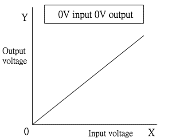 | 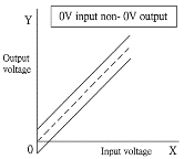 |
| (Fig. 202) 0V input 0V output | (Fig. 203) 0V input non-0V output |
Reading error
For a digital multi-meter, DMM, there is no need to set the instrument initially to zero, as its built-in electronic circuit has already incorporated a nulling device. However, if the DC 2000 mV full scale range is selected, one will find the initial reading is not steady and fluctuates, compared with the DC 20 V FS range. This cannot be avoided as the instrument is set to a high impedance input mode which is sensitive to environmental noise signals. For a moving needle multi-meter, when set to measure resistance, the set zero knob (Fig. 204) has to be adjusted to make the needle rests at the 0 W position. Also, for voltage measurement, the panel meter has a small trimmer which can be hand-adjusted by a small screw driver to make the pointer rests at 0 V (Fig. 205).
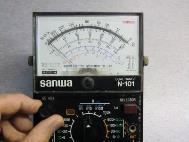 | 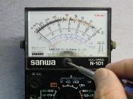 |
| (Fig. 204) Ohm set zero knob | (Fig. 205) Hand adjustment to voltage zero |
A flow chart of sensor-based instrumentation:

Take, for example, the case of pH measurement by glass electrode. A glass electrode cannot be directly fed to a DMM for e.m.f. (or calibrated as pH) measurement, because the output resistance of glass electrode and input resistance of the DMM do not match. A glass electrode has an output resistance of about 1012 Ω while a DMM has an input resistance of only 10 MΩ. A sensor has to be used between the two devices for output/input resistance matching. When a probe/sensor combination is connected to a DMM, the resulting combination, on top of the input/output resistance matching, the probe/sensor combination also has to be designed to fulfill the condition of 0V input / 0V output. Usually a senor employs either (i) an external nulling circuit or (ii) an internal nulling circuit.
(v) Linear amplification after nulling
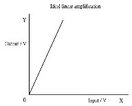
(Fig. 206) Ideal linear amplification
No matter a low (less sensitive) or a high input resistance (more sensitive) instrument is used, it should be set to a 0 V initial condition.
As shown in Fig. 206, in order to have direct proportional amplification, the straight line of the graph should pass through the (0, 0) point. Setting the sensor to initial input 0V can be achieved by either (i) external nulling, i.e. circuit outside the IC or (ii) internal nulling. i.e. the IC provides pins for nulling.
(vi) External buffered input nulling – low input resistance sensor (< 10MΩ)
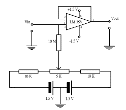
(Fig. 207) External nulling
A buffered circuit is in fact a simplified version of non-inverting amplifier, in which the (-) input and the output terminal is short-circuited (Topic 8.3.2 part c, Fig. 220). Voltage gain is calculated as follow
Vout = Vin (1 +![]() ) or Vout = Vin (1 +
) or Vout = Vin (1 + ![]() ),or Vout = Vin i.e. no voltage gain.
),or Vout = Vin i.e. no voltage gain.
Two 1.5 V dry cells are connected in series as shown in Fig. 206 to generate a dual (+) and (-) power source. Pin 8 of LM 358 is connected to +1.5 V and pin 4 to -1.5 V. The series resistors 10 K (x2) and 5 K act as a potential divider for a 3V potential. The junction of the two dry cells is connected to ground and provides a +1.5 V and -1.5 V power supply. Adjustment of the 5 K variable resistor provides positive, zero and negative voltages.
The (+) input of IC, through the 10 M resistor, is connected to this potential divider combination. This is a typical way of connecting an Op-Amp to function as a non-inverting amplifier. When the 5 K variable resistor is adjusted so that Vout = 0 V, the condition of 0 Vin / 0 V out condition is achieved and the position of 5 K variable resistor knob is fixed. This way of nulling input offset is called external nulling. After this set zero procedure, an input of 1.00 V will display an output of 1.00 V, or Vin = Vout, i.e..no voltage gain. Input resistance of the IC is 10 MW and output resistance is 0 W (characteristic of an ideal Op-Amp).
One major advantage of using LM 358 is that it is a single power supply IC, i.e. it needs only a positive voltage supply, does not need a negative voltage supply. Hence a dual power supply circuit for LM 358 is not common. Single power supply provides no negative voltage, external nulling for an Op-Amp non-inverting amplifier is not possible. Hence the IC needs only one resistor (bias resistor) to be connected to the ground at the (+) input for tapping a p.d. to make the potential at the (+) input equal to that at the (-) input, one of the characteristics of an ideal Op-Amp. This resistance serves as the input resistance of the IC. For LM 358, input resistance is not too high and a 10M resistor is suffice. If the 10 M bias resistor is connected, the minute bias current will reestablish a p.d. at pin 3 such that Vin is almost equal to Vout. The Circuit for a single power supply and buffered input for LM 358 is shown in Fig. 208. As the p.d at the (+) input is supposed to be equal to that at the (-) input and allowing for a slight deviation due to lack of nulling, Vin = Vout is by and large achieved.
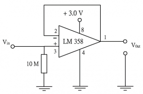
(Fig. 208) A single power supply buffered input circuit of LM 358
Project (8):Dual / single power supply buffered input for LM 358
Material: LM 358, breadboard, 1.5 V dry cell with battery cap (x2), 10 K (x2),1 K variable resistor, (resistor 10 M, 100 K and 10 K @), DMM
Procedure:
(1) Connect all components as illustrated in Fig. 206 on a breadboard. Adjust the 5K variable resistor until Vout = 0 V, keep the position fixed. Complete the following table.
Input resistance/Ω | Vin/V | Vout/V | Input resistance/Ω | Vin/V | Vout/V |
10M | 0.00 | 0.00 | 10M | 200.0 mV |
|
100K | 100K |
| |||
10K | 10K |
| |||
1K | 1K |
|
(2) Connect all components as illustrated in Fig. 208 on a breadboard and complete the table below:
Input resistance/Ω | Vin/V | Vout/V |
10M | 1450 mV |
|
100K |
| |
10K |
| |
1K |
|
Conclusion:
For the first experiment, as the input resistance changes from 10 MΩ to 1 K Ω, Vout is almost equal/equal to 200 mV. For the second experiment, as the input resistance changes from 10 MΩ to 1 K Ω, Vout is almost/not equal to 1450 mV. 10 M input resistor gave the _______ output deviation. For LM 358 Op-Amp and using 10 MΩ input resistance, as far as the condition Vin = Vout is required, the dual power supply buffered input method and the single power supply buffered input method makes __________ difference.
(vii) Internal buffered input nulling – high input resistance sensor (> 1010 Ω)
Laboratory pH meters are all made with glass electrodes. In order that measurement can take place, the thin special glass membrane has to conduct a necessary tiny amount of current. Glass is a well-known poor conductor of electricity which means it has an extremely high electrical resistance (1014 Ω per meter). Glass combination electrode generates an e.m.f. of about 1 V, and according to ohm’s equation I = V/R, a glass membrane of about 0.1mm thick has a resistance of roughly 1010 Ω. Under such condition, current through the membrane is less than 10-10 A or 100 pA. Hence an Op-Amp with an input resistance of at least 1010 Ω or 10000 MΩ is required for initial amplification. High impedance and noise closely associated together. In order that instrument can be steadily operated, the input should be under a low impedance environment. Input stage employing voltage follower buffer is a good design for the purpose. Voltage follower can lower noise signal, very suitable for accepting high impedance probe outputs.
A general purpose LM 358 is far from suitable for the job. High input impedance Op-Amp with FET input stage like CA 3130 or LF 356 is generally used. Nowadays fabrication technique enables IC not using FET input stage can also handle high resistance sensors, like the low temperature drift Op-Amp OP-07, OP-27 etc
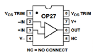 | 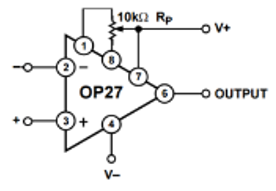 |
(Fig. 209) OP 27 pin arrangement | (Fig. 210) Dual power internal nulling |
Project (9): Dual power source high input resistance buffered follower using OP-07
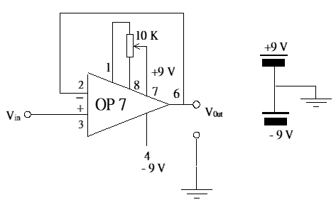
(Fig. 211) OP-07 Voltage follower
Material: OP-07,breadboard, 9V dy cell with battery cap (x2), 10 K variable resistor, DMM,1.5 V (x2) dry cell with battery cap
Procedure: Connect all components as illustrated in Fig. 211 on a breadboard. Adjust the 10K variable resistor until Vout = 0 V, keep the position fixed. Feed 1.5 V and 3.0 V to the (+) input of the IC. Complete the following table.
| Vin | Vout | Input e.m.f. | Vin | Vout |
| 0 | 0 | 1.50 V | 1500.0 mV | |
| 0 | 0 | 3.00 V | 3000.0 mV |
Irrespective of the nature of amplifying circuit, an initial buffered voltage follower input design is a decent method of screening unwanted analogue noise signals.
(viii) Nulling by installing a bias resistor
For inverting Op-Amp amplifiers, the observed 0V in ≠ 0V out situation due to unequal p.d at the (+) and (-) inputs (i.e. input offset voltage) is usually corrected by installing a resistor, called the bias resistor, at the (+) input as shown in Fig. 219. Description of this method of nulling will be mentioned on page 91.
(ix) Power source of OP-Amp
Most Op-Amps feature dual power supply. The pin connecting the positive pole of the power source is called Vcc (or Vdd for CMOS), the pin which is made negative is called Vee (Vss for CMOS). Like LM 741, the least supply voltage is ±5 V. Dual power supply requirement is not convenient for portable electronic devices. Nowadays single power supply IC is quite popular. These Op-Amps need supply voltage as low as 3 V, like LM 358 (dual) or LM 324 (quad). A 3 V button-like lithium battery enables LM 358 circuits to function properly. Portable and convenient to use are usually selling points of electronic appliances.
(x) Packaging of Op-Amp
Mainstream Op-Amps are almost all packed with a DIP (dual-in-line package) finish. IC leads protrude from both sides of the package. Plastics is the most common packaging material, i.e. PDIP. Dual array direct insert IC either inserts into a socket or soldered onto a circuit board. Op-Amp chips are seldom available as single units, they are often packed with dual or quad units fabricated in the same package (Fig. 212, 213).
 |  |
(Fig. 212) Dual unit LM 358 | (Fig. 213) Quad unit LM 324 |
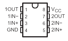 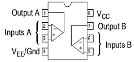 |   |
| (Fig. 214) LM 358 pin assignment | (Fig. 215) LM 324 pin assignment |
(b) Ideal and non-ideal operational amplifiers
Technical definition of an ideal and a non-ideal Op-Amp can be searched from the internet. Amateur electronic hobbyists may find it difficult to fully understand. Hence a table summarizing the features (linear amplification only) of ideal and non-ideal behavior is desirable for a simplification of difficult concepts.
| Ideal Op-Amp (for calculation) | Non-ideal (practical) Op-Amp for circuit designs | |
| 1 | 0V input, 0V output (no output offset voltage) | Slight voltage output even if there is no signal source. The voltage applied at the (+) and (-) inputs to bring 0V output is called the input offset voltage. Usually it is very small, in the order of mV. |
| 2 | Open loop (+ and – inputs not connected) condition has infinitely large voltage gain. | Open loop gain of a real Op-Amp can be very high, but not infinite. |
| 3 | Potential at the (+) input and the (-) input are the same. If the (+) input is connected to ground (0V), the (-) input is assumed to be at 0V, even though it is not. The (-) input under this condition is called “virtual ground”. | Some p.d is developed between the (+) and (-) inputs (input offset voltage). Ideal behaviour can be approached by installing a bias resistor at the (+) input to generate a p.d. that matches the (-) input. |
| 4 | No current flows between the (+) and (-) inputs. | Current flowing into/out the (+) input (bias (+) current) and current flowing into/out the (-) input (bias (–) current) are not equal. The difference is called input offset current. |
| 5 | Infinitely high input impedance, will not load the signal source. Experimental results are expected to be the same as theoretical results. | Bipolar input Op-Amps normally do not have high input resistance, 10 MΩ. or something like that. However. FET input Op-Amps can offer input resistances up to 1.5 TΩ. Even so, it is still not infinite and still loads the source. Experimental results deviate from theoretical results. |
| 6 | Zero output resistance, current generated can all be fed to the next stage. | Op-Amp calculations usually do not involve output resistance. Op-Amp amplifies voltage, not current. Output parameter is voltage. Take for instance, an output of 3 V, (i) if the output is short circuited to ground (or zero load resistance), output is still 3 V but will activate the protective device. (ii) if the loading resistance is 1000 Ω, and according to V = iR, the next stage will consume 3 mA current and the input resistance of the Op-Amp of next stage is regarded as 1000 Ω. |
Calculations of Op-Amp circuits are all based on the Op-Amp behaving ideally. In practice, all Op-Amp deviate from ideal behavior and causes various types of bias. For example, input bias current, input offset current, input offset voltage, drift etc. They can be eliminated by suitable designs of relevant circuits as described earlier (related information obtainable from the internet).
8.3.2 Practical Op-Amp circuits
(a) Linear amplification
From a basic graphical analysis point of view, a proportional straight-line graph should pass through the (0, 0) OX and OY axis origin (Fig. 216). Slope of the graph (m) is the magnification multiple. If the straight line does not pass the origin, an intercept (b) on the OY axis occurs, making y’ to be the OY axis value, in which y’ = y + b where y is the ideal value (Fig. 217). If b is small, situation approaches the ideal value.
 |  |
| (Fig. 216) Ideal proportional straight-line thro the origin | (Fig. 217) Intercept b and deviation from ideal value |
Fig. 216 and 217 nicely apply to linear amplification by Op-Amps. Let the OX axis be the input voltage and the OY axix be the output voltage, an ideal Op-Amp suits the situation of Fig. 216, and satisfies the 0Vin / 0Vout condition. Non-ideal Op-Amp behaves like Fig. 217 and will have an offset voltage b when there is no input. b value is usually very small, in the order of a few milli volt. However, it cannot be ignored and should be eliminated when considering the following coupled stages of electronic designs.
(b) Closed loop inverting amplifier
Closed loop inverting amplification means (i) source signal is fed to the (-) input, (ii)
a negative feedback resistor is installed between the output and the input and (iii) the sign of the output voltage is opposite to that of the input voltage. A typical Op-Amp inverting amplifier is shown as below:
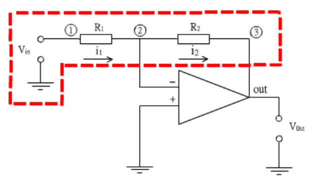 (Fig. 218) A closed loop inverting amplifier
Calculation is based on an ideal Op-Amp which signifies the p.d. at the (+) and (-) inputs are the same. The (+) input is connected to ground (0V), but (-) input is not connected to the ground, therefore the p.d at this point cannot also be 0V. However, as abided by the ideal behaviour criterion for calculation, the (-) input has to be looked upon as having 0V, hence it is called “virtual ground”. With reference to the red frame in Fig. 218, we have:
V = i1R1 + Vin
Where V = 0 and i1 = i2 as no current is assumed to flow through the inputs. Hence
![]()
voltage gain = (![]() )
)
or Vout = -Vin (![]() )
)
Vout = i2R2 + V
Project (10 ):By using available components, complete the circuit as shown in Fig. 218
Material: DMM, breadboard, 1.5V, 3.0V, 4.5V power supply, LM 358, 1K, 2K, 10K resistor, connecting wires, crocodile clips
Supply voltage (Vcc) = _______ V
| (+) input voltage | (-) input voltage | Output voltage |
| 0 V | 0 V | ( ) V |
Input voltage Vin | R1/Ω | R2/Ω | Calculated Vout | Observed Vout | ||||
negative | 1.5V | 0 | 0 |
| = 0 |
| ||
1K | 1K |
| = |
| ||||
1K | 2K |
| = |
| ||||
1K | 10K |
| = |
| ||||
3.0V | 0 | 0 |
| = |
| |||
1K | 1K |
| = |
| ||||
1K | 2K |
| = |
| ||||
1K | 10K |
| = |
| ||||
Input voltage V in | R1/ Ω | R2/ Ω | VR1 | Vout = (Vin+VR1+VR2) | Observed Vout | |
positive | 1.5V | 0 | 0 |
|
|
|
1K | 1K |
|
|
| ||
1K | 2K |
|
|
| ||
1K | 10K |
|
|
| ||
3.0V | 0 | 0 |
|
|
| |
1K | 1K |
|
|
| ||
1K | 2K |
|
|
| ||
1K | 10K |
|
|
| ||
Conclusion:
(i) When the power supply of LM 358 is ______ V, open-loop saturated output voltage (Vsat) is ________ V.
(ii) When connected to a negative input voltage, output voltage is basically _______
times the negative input voltage, resulting in a __________ voltage.
(iii) Because of interactions, Practical Op-Amps (non-ideal) do have small amount of current flowing through the two inputs, called input bias current. Voltage gain calculation assumes same p.d. at the two inputs and hence arrive at a value of Vout. In reality the p.d. at the (-) input is not the same as that of the (+) input or 0 V, hence its name “virtual ground”. Thus, a means of correction is required to generate a p.d. at the (+) input to match that of the (-) input. The method is to connect a bias resistor R3 between the ground and the (+) input to develop a p.d (refer to the diagram below). The value of R3 is equal to the parallel resistance of R1 and R2, i.e. R3 = (R1 x R2) / (R1+R2). For more details of correction for input bias current, you can view professional information from the internet. In addition, high impedance input FET Op-Amps do not need such correction, especially in the non-inverting amplification mode.
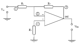
(Fig. 219) Installing a bias resistor R3 for a closed loop inverting amplifier
(iv) When connected to a positive input voltage, the output voltage becomes positive, not negative. This is illustrated by using the formula of (Vin + VR1 + VR2) = Vout. If R2 is a light-depending resistor (LDR), the change of value of resistance upon variation of wave-length and intensity causes a change in Vout. This is the basic principle of colorimetry. Program (2) will have a detailed description of the technique of “DMM display” with respect to this kind of application.
(c) Closed loop non-inverting amplifier
Close loop non-inverting amplification means (i) source signal is fed to the (+) input, (ii) feedback serial resistors (in fact a potential divider) is installed between the output, the (-) input and the ground and (iii) the sign of the output voltage is the same as that of the input voltage. A typical Op-Amp inverting amplifier is shown as follows:
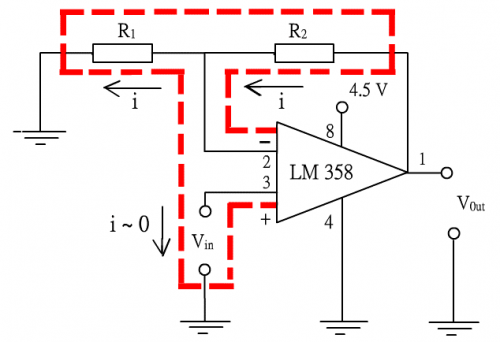
(Fig. 220) Close loop non-inverting amplifier
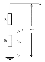
(Fig. 221) Equivalent circuit of a close loop inverting amplifier
An ideal Op-Amp assumes no current flows through the two inputs, therefore current thro R1 = current thro R2 (Fig. 220, red frame). According to the equivalent circuit of (Fig. 221),
![]() ) = (
) = (![]() )
)
Voltage gain = (1 +![]() )
)
or Vout = Vin (1 +![]() )
)
Unlike inverting amplifier, non-inverting amplifier, apart from normal voltage gain, can also have 0 voltage gain. According to the formula Vout = Vin (1 +![]() ), substituting R2 = 0,R1 = ∞ arrives at Vout = Vin, or 0 V input, 0 V output. 1 V input results in 1 V output etc. It seems equivalent output carries little importance, but the screening and buffer effect is commonly adopted as the initial stage of amplification. The result is exactly the same as a buffer voltage follower (refer to page 80):
), substituting R2 = 0,R1 = ∞ arrives at Vout = Vin, or 0 V input, 0 V output. 1 V input results in 1 V output etc. It seems equivalent output carries little importance, but the screening and buffer effect is commonly adopted as the initial stage of amplification. The result is exactly the same as a buffer voltage follower (refer to page 80):
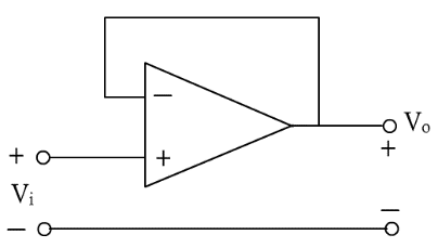
A voltage follower
The net result under this condition is convert a high resistance signal source voltage (vulnerable to noise interference) to the same voltage output but with almost zero output resistance (free from noise interference).
A must-use application is found in circuit design for glass electrode in pH measurements. Glass electrode has extremely high resistance (~1012Ω), and source signal outputs only ~10-12A. Once connected to a consumer DMM as shown in Fig. 222, the relatively low input resistance of the DMM will withdraw an appreciate amount of current from the signal source to sustain a significant voltage which is much lower than the e.m.f. of the signal generated from the glass electrode. As a result, the measured voltage is much lower than the expected e.m.f. output of the glass electrode or the instrument lacks sensitivity. The usual correction for this mismatch of resistance is to use a high input resistance FET Op-Amp like CA 3130 as the initial stage of amplification.
b. Probe output resistance and instrument input resistance
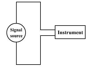 | 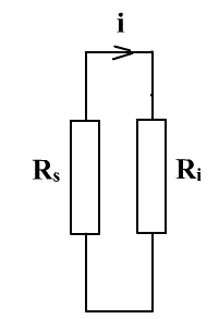 |
(Fig.222) High input resistance signal source and input resistance of the instrument connected in parallel
Resistance of the probe and the input resistance of the instrument can be looked upon as two resistors connected in parallel:
![]()
High impedance input non-inverting amplifier is usually employed as the input stage of the sensor prior to the amplification stage, because it can handle weak analogue source signals. Resistance of the probe and the input resistance of the instrument can be looked upon as two resistors connected in parallel:
A brief summary:
| Rs (probe) | |||
| Very high impedance | Low impedance | ||
| Ri(instrument) | Very High impedance | Little effect on e.m.f. of signal source | E.m.f. of signal source (iRs) not much affected, as available i shares little by the instrument (load). |
| Low impedance | E.m.f. of signal source (iRs) greatly affected (decreased), as appreciable amount of available i is drawn by the instrument (load) which causes the e.m.f. of the probe to drop greatly. | Little effect on e.m.f. of signal source | |
(d) Comparator (non-linear application)
Linear operation of an Op-Amp assumes ideal behavior in which one of the assumptions is based on the (+) and (-) inputs are of the same potential or at 0V p.d. Non-linear operation, on the contrary, is based on the two inputs have different polarity or potential difference so as to undergo mathematical functions other than simple proportionality.
As its name implies, an operational amplifier functions not only as a linear amplifier (voltage multiplication), but is also able to perform other non-linear mathematical functions. Operation is a mathematical term which has a lot of definitions.
A layman of electronic professional expertise may look upon an Op-Amp as two individual dc amplifiers, the (+) input accepts one signal while the (-) input accepts another. In actual fact, even if one input accepts signal, the other input will be activated. In other words, states of the two inputs must be considered at the same time, irrespective of which input is involved. Condition as such creates the outstanding function of an Op-Amp as a mathematics-oriented multi-functional electronic device. Traditional multiplication (as a linear amplifier) as well as non-linear functions like generation of sine waves, square waves, saw-tooth waves, integrations, differentiations, filters, comparators, oscillations, A/D and D/A conversions, timer etc are well-designed by circuit developers.
One non-linear function which relates closely to digital computation is an Op-Amp comparator. A basic comparator works on the principle of simultaneously comparing the magnitude of the (+) and (-) input signals and at the same time outputs a saturated voltage. The term (Comparator) literally means comparing two voltages and then decide a fixed (saturated) output.
A simple Op-Amp comparator generating pulse signal outputs
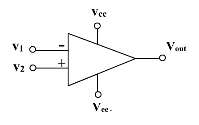
(Fig. 223) Open-loop state
Consider an open loop (no negative feedback connection) Op-Amp assembly with the (+) and (-) inputs left open (Fig. 223). Connection as such is very unstable, as open loop voltage gain is extremely high. If the p.d. at the (+) input V2 is above the p.d. at the (-) input V1, the extremely high voltage gain will output a saturated voltage +Vsat. Conversely, a -Vsat voltage also appears if the p.d. at the (-) input V1 is above the p.d. at the (+) input V2. Set-up of an Op-Amp LM 358 connected as a comparator as illustrated in Fig. 224.
| Source signal | Vout | |
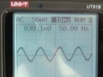
30 mV 50 Hz sine wave | 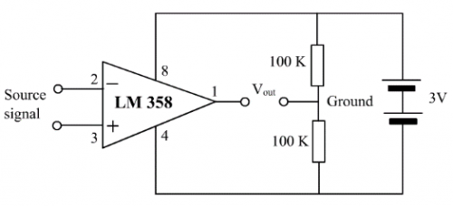 |
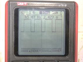
1.04 V 50 Hz square wave |
| (Fig. 224) An Op-Amp comparator |
When the (+) and (-) inputs are connected to a low AC 50 Hz 30 mV sine wave signal source, the only instant when the inputs and the output are of the same voltage is when the sine wave chain is at the 0V time line. The sinusoidal propagation of +30 mV thro 0 V and -30 mV periodically changes 50 times per sec. Once the voltage of, say, the (+) input is just above that of the (-) input, the open loop voltage gain boosts the output to +Vsat and vice versa. As a result, a continuous square wave voltage pulse chain will appear at the output. Vout detected a 1.04 V 50 Hz square wave form. In general, for Op-Amp IC, Vsat = (Vcc – 0.5 V) and the observed 1.04 V agrees with the expected value. One point to note is that the “ground” of the circuit of Fig. 223 is not the negative pole of the 3 V battery, it is instead the point of the intersection of the two 100K series resistors dividing the poles of the 3 V battery. Hence Vcc at pin 8 is + 1.5 V and not 3 V and Vee at pin 4 is – 1.5 V.
The above example is a simple external activated (AC sine wave) square wave oscillator based on an open loop Op – Amp comparator. However, nearly all signal generators (oscillators) have built-in self-starting design and would not adopt AC power supply frequency as time base. The following relaxation oscillator is a popular example of free running (self-starting) multi-vibrator.
(e) Oscillation (non-linear application)
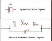
Oscillation belongs to a kind of multi-vibrations. The most important application of multi-vibration is to provide a time base, a frequency counter or simply a clock. Small gadget like wrist watch or complicated machine such as computer requires very accurate time base. These devices all use mechanical resonance of a vibrating quartz crystal of piezoelectric material to create an electrical signal with a precise frequency as accurate as 14,318,180 Hz (Fig. 225, 226, 227).
 |
 |
 |
| (Fig. 225) A 12 MHz quartz crystal | (Fig. 226) Circuit symbol for quartz |
(Fig. 227) Clock assembly of a computer |
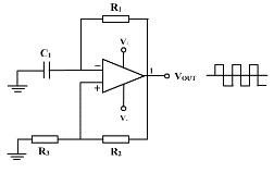
(Fig. 228) A typical relaxation oscillator
Circuit analysis of Fig. 228 can be done as follows:| The circuit on the right can looked upon as a RC charge/discharge loop, generating a negative feedback, thro R, to the (-) input. It then follows by a positive feedback by tapping the mid-point of R+R potential divider at the (+) input. Operation is based on the Op-Amp functioning as a comparator. | 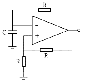 | |
| (a) The (+) and (-) inputs of a comparator is verysensitive to change of p.d. The output would not stay at 0V once power supply is connected. At a certain instant when the (-) input has a more negative potential than the (+) input, the comparator function is activated and the output becomes +Vsat (invertedly amplified). Right after this, (i) the capacitor is charged through the negative feedback resistor R and (ii) the (+) input is changed temporarily to +Vsat/2 (positive feedback of the output through the mid-point of the R+R potential divider). The (-) input becomes positive as a result of capacitor charging. When the potential of the (-) input is more positive than +Vsat/2, the comparator mechanism is again activated and the output immediately becomes -Vsat. | 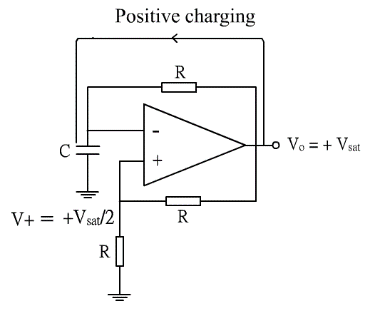 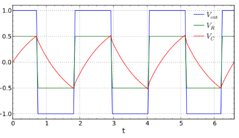 | |
| (b) When Vout = -Vsat, the (+) input becomes -Vsat/2, again through positive feedback. The capacitor starts to discharge as the (-) input is made negative. As the (-) input becomes more negative than -Vsat/2, the comparator function is again activated and the output immediately changes to +Vsat. | 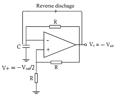  | |
Steps (a) and (b) repeat unlimitedly and as a result, the ouput of the IC appears a square wave pulse chain (blue line), see also Fig. 231. While the (-) input and the ground detect a chain of saw-tooth wave (red line, see also Fig. 230).
Relaxation oscillation
(iv) LM 358 relaxation oscillator
A single power supply Op-Amp LM358 offers a lot of convenient applications more than other dual power supply Op-Amps. Fig. 229 is a typical LM 358 relaxation oscillation circuit based on comparator function.
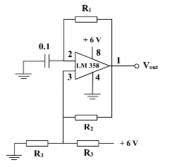
(Fig. 229) Single power supply LM 358 relaxation oscillator
![]()
If R1 = 150 K, R2 = 150 K, R3= 100 K,frequency of square wave
![]() Hz=
Hz= ![]() = Hz = 50 Hz
= Hz = 50 Hz
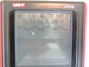 |
 |
| (Fig. 230) Saw-tooth wave detected between pin 2 and ground |
(Fig. 231) Square wave detected between pin 1 and ground |
Program (2) Topic 5.2 provides a relaxation oscillator circuit used by a self-devised conductance meter for generating AC wave form for electrical conduction of aqueous solution that avoids electrolysis.
8.3.3 Applications of voltage regulators
(i) Why voltage regulation?
Dry cell is the only convenient portable power supply for electronic appliances. Long period usage will lead to drop of level of voltage supply. The result greatly affects the performance of the appliance and will eventually make it unworkable. Ideally speaking, voltage supply upon loading should maintain at the same level for a period as long as possible. The situation usually overcomes decently by using alkaline batteries. If components of the device mainly use IC chips, which consume little current and can maintain performance over a long period of attenuating voltage, the problem is not so acute. Of course, the ideal case is worth looking for, especially in operating mechanical devices like portable electric motor or maintaining a steady level of light source like a portable colorimeter. Drawbacks as such are usually corrected by using voltage regulators.
(ii) Consumer voltage regulator IC
Voltage regulators are popular purchasable electronic components. Consumer fixed voltage regulating ICs include:
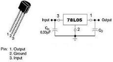
(1) 78XX series. These are positive voltage regulators. Regulated voltage ranges from +5.00 V, +6.00 V, +8.00 V…to 24.00 V. Delivers current outputs from 1.5 A (package TO – 220 Fig. 231), 500 mA (the M series, package TO – 220) and 100 mA (the L series, package TO – 92, Fig 232). All have built-in short circuit protection device.
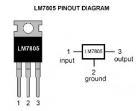 |
 |
| (Fig. 232) TO-220 | (Fig. 233) TO-92 |
(2) 79XX series. These are negative voltage regulators. Regulated voltage ranges from -5.00 V, -6.00 V, -8.00 V…to -24.0 0V. Current output and packaging form the same as the 78XX series.
The internal structures of voltage regulator ICs are complicated (Fig. 234), but the pin layouts are very simple, all provide with 3-pin arrangement (Fig. 232, 233), making soldering straight forward and easy. One important feature of voltage regulators is that the voltage to be regulated (input voltage), must be higher than that of the desired regulated voltage (output voltage). For example, a DC 5.00 V regulated voltage power supply must receive an incoming unregulated voltage higher than 5 V. The difference normally should not be less than 1.5 V. Using 7805 to regulate a 9 V dry cell power supply to provide a stable DC +5.00 V voltage source for long term loading is a smart way of power consumption management.
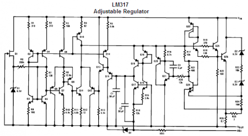
(Fig.234) Internal structure of LM 317
(iii) Adjustable voltage regulator
These voltage regulator ICs are becoming more and more popular. Available adjustable voltage regulators also provide positive (the LM 317 series) and negative (the LM 337 series) voltage regulations. Packaging of LM 317 has the T (TO – 220), the M (TO – 220) and the L (TO – 92) series (Fig. 235), delivering current outputs of 1.5 A, 500 mA and 100 mA respectively. Output voltage can be as low as ± 1.25 V to ± 37 V, freely adjustable. A first-choice voltage regulation method for portable low voltage electronic appliances.
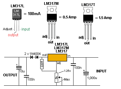
(Fig. 235) Packaging of LM 317
(iv) Applications of LM 317
Available LM 317 is usually in the form of TO – 220, LM 317T (1.5 A) packaging.
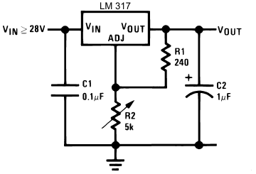
Practical circuit of LM 317 is quite standardized. Nealy all adopted the following circuit for various applications:
 |
 |
| (Fig. 236) Standard LM 317 voltage regulation circuit | |
C1 and C2 can be disposed of if the power supply comes from a dry cell or battery. LM 317T outputs regulated voltage from 1.25 V to [1.25 x (1+ R2/R1) ] V.
- If Vin = 29 V, R1 = 240 Ω and R2 = 5 K Ω, maximum output voltage = [1.25 x (1+R2/R1) ] V, or 27.3 V。
- The input voltage should be 1.5 V above the regulated voltage and this means in this case, the input put voltage should be at least 29 V or more in order to obtain a regulated voltage of 27.3 V.
- If R2 = 0 Ω,regulated output voltage = [1.25 x 1 ] V or 1.25 V.
- Therefore, by adjusting the variable resistor of 5 KΩ, regulated voltage changes from 1.25 V up to 27.3 V for an input of 29 V.
- Keeping R1 but changing R2 to 1 KΩ , the maximum regulated voltage is [1. 25 x (1 + 1000/240) ] V or 6.46 V and the input voltage is at least (1.5 + 6.46) V or 7.96 V. A 9 V dry cell will suffice.
- Similarly, Keeping R1 but changing R2 to 500 Ω, the maximum regulated voltage is [1.25 x (1 + 500/240) ] V or 3.85 V and the input voltage is at least (1.5 + 3.85) V or 5.3 5 V. A 6 V dry cell will suffice.
Summarizing voltage regulation by LM 317:
| Fixed resistor (R1) | Variable resistor (R2) | ||||||
| 240 W |
[1.25 x (1+ R2/R1) ] V |
5K Ω | 1K Ω | 500 Ω | |||
| Input voltage | Regulated voltage | Input voltage | Regulated voltage | Input voltage | Regulated voltage | ||
| ≥ 29 V | (1.25 – 27.3) V | ≥ 7.96 V | (1.25 – 6.46) V | ≥ 5.35V | (1.25 – 3.85) V | ||
Topic 14 involves the construction of a mini magnetic stirrer. The circuit used employs a regulated voltage to drive a mini motor. The method is superior than using a simple resistor-motor in series combination. Program (2) Topic 5.3 describes the construction of a portable colorimeter using a tricolor LED as near monochromatic light source, the power for the light source is a regulated voltage supply which enables the LED perform a long-term light emission without attenuation.

